By STMicroelectronics 201
TIP3055 is an NPN power transistor commonly used in amplification and switching applications.
TIP3055 is a silicon epitaxial INPN transistor using TO-218 stretchable package. It is an ideal device for power conversion circuits, parallel or series control (voltage regulators), output phase and high power amplifiers. The corresponding one is TIP2955. This product is widely used in many industrial projects that require sound amplification. It's identical in construction, but the maximum power indulgence is slightly smaller.

Ⅰ.Specifications of TIP3055
•Number of pins:3
•Configuration:Single
•Transistor polarity:NPN
•Installation style:Through Hole
•Package/Box:TO-247-3
•Product Category:Bipolar Transistor-Bipolar Junction Transistor (BJT)
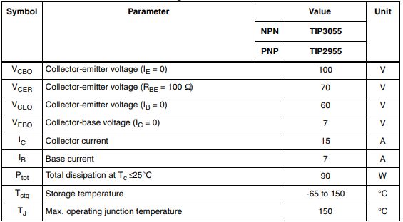
•Emitter-base voltage VEBO:7 V
•Collector-emitter saturation voltage:1 V
•Maximum DC collector current:15 A
•Collector-base voltage VCBO:100 V
•Collector-emitter maximum voltage VCEO:60 V
•Height:20.15 mm
•Width:5.15 mm
•Length:15.75 mm
•Pd-Power dissipation:90 W
•Minimum operating temperature:-65℃
•Maximum operating temperature:+150℃
•Collector continuous current:15 A
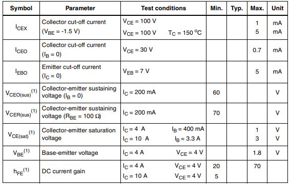
•Maximum DC current gain hFE:70
•DC collector/Base Gain hfe Min:20
•Current -collector cutoff (maximum):700µA
•Breakdown voltage (collector-emitter):60 V
•Minimum current amplification (hFE):20 @4A, 4V
•Vce saturation voltage drop (maximum value) when Ib and Ic are different:3V @ 3.3A, 10A
Ⅱ.Application circuit of TIP3055
1.Amplification circuit: This is a simple amplification circuit using TIP3055 as the output stage of the amplifier. The signal is coupled to the base through the input capacitor C1, and R1 and R2 form a voltage divider network to determine the base voltage. C2 is the DC coupling capacitor for the output signal, while R3 is used to provide feedback.
2.Switching circuit: This is a simple switching circuit used to drive a relay. When the input signal is passed to the TIP3055 through R1 and the base, the TIP3055 conducts, passing current to the relay and causing it to close. R2 is to ensure that the base voltage of the TIP3055 is at the appropriate level.
3.Bias and power supply: In order to ensure the normal operation of TIP3055, appropriate bias voltage and power supply need to be provided.
4.Output signal processing: C2 is the DC coupling capacitor of the output signal, which is used to isolate the DC and AC components of the output signal.
Ⅲ.Working principle of TIP3055
•The working principle of TIP3055 is based on the amplification principle of silicon NPN transistor. When the input signal is coupled to the base through the input capacitor C1, the base current IB changes, which in turn causes the collector current IC to change. Since there is a certain amplification relationship between the collector current IC and the base current IB, the input signal is amplified through the amplification circuit and output to the load.
•In the application circuit of TIP3055, the voltage divider network composed of R1 and R2 is used to adjust the base voltage to control amplification and stability. R3 provides feedback to further control amplification and stability. C2 is the DC coupling capacitor of the output signal, used to isolate the DC and AC components of the output signal.
•It should be noted that the specific circuit design and parameters need to be determined according to the application needs and circuit requirements. At the same time, in order to ensure the stability and performance of the circuit, proper testing and verification are also required.
Ⅳ.Temperature performance of TIP3055
1.Temperature range: Check the data sheet to understand the operating temperature range of the TIP3055. Make sure the application does not exceed this range. If you need to operate in a high-temperature environment, you may need to choose components with a wider operating temperature range. The general operating temperature range is -65℃~150℃.
2.Temperature compensation: Some applications may need to consider the impact of temperature on component performance. Consider using temperature compensation circuitry in your design to ensure good performance is maintained at different temperatures.
3.Heat dissipation design: In high temperature environments, heat dissipation becomes more important. Make sure to provide adequate heat sinking for the TIP3055 to prevent overheating. This may include the use of a heat sink or fan, depending on the requirements of the application.
4.Stability: Temperature changes may cause performance fluctuations in electronic components. In high-temperature environments, make sure your design is stable enough to not be overly affected by temperature.
5.Package type: Different package types may have different adaptability to high temperature environments. Make sure the package you select meets your application needs.
Ⅴ.Connection method of base and collector of TIP3055
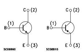
1.Pin 1(Base): Connected to the control input, usually an input signal or drive signal. By applying a forward voltage to the base, the conduction of the transistor can be controlled.
2.Pin 2(Collector): Connect to the source of load current, usually the output of the supply current. This is where the current flows into the transistor.
3.Pin 3(Emitter): Connect to the sink of the load current, usually ground. This is where the current flows out of the transistor.
Basically, the base of the TIP3055 (pin 1) controls the current flow to determine the current flowing between the collector (pin 2) and the emitter (pin 3). Under normal operating conditions, by applying a certain forward voltage to the base, current flows from the collector to the emitter, thereby turning on the transistor. When the voltage at the base decreases, the transistor is turned off and current cannot flow.
Ⅵ.Absolute maximum rating of TIP3055
Ⅶ.Electrical characteristics of TIP3055
(Tcase=25 °C;unless otherwise specified)
Ⅷ.Method to adjust the variable voltage and variable current limit of TIP3055
•Adjust current
1.Base control: By applying a forward voltage to the base (pin 1) of the TIP3055, the conduction of the transistor can be controlled. This voltage is usually provided by connecting to a control circuit or resistor divider network.
2.Load resistance: Load resistance also affects the adjustment of current. By adjusting the size of the load resistor, you can adjust the output current.
3.Current limiting resistor: Between the collector (pin 2) and emitter (pin 3) of the TIP3055, you can use a current limiting resistor to set the output current. This resistor is usually connected to the collector.
4.Current limit protection: Some applications may require additional current limit protection circuitry to ensure that the output current does not exceed the required range.
•Precautions
1.Data sheet: Be sure to consult the TIP3055 data sheet for detailed information on operating parameters, limits, and recommended circuits.
2.Stability: Pay attention to the stability of the system when adjusting the current to prevent current fluctuations from causing problems.
3.Heat dissipation: When adjusting the current, make sure that the TIP3055 is within a safe operating temperature range. If the current is larger, it may be necessary to provide appropriate heat sinking.
Ⅸ.General usage of TIP3055 in circuits
1.Current source: TIP3055 can be used as a current source. With proper circuit design and connections, the TIP3055 can be configured as a stable current source to drive a variety of loads. To implement the TIP3055 as a current source, it is usually necessary to connect it to an appropriate resistor network. This resistor network is used to adjust the output voltage of the TP3055 to the desired value and ensure that the current through the resistor network remains constant. In order to obtain a stable current source, appropriate resistor values and resistor network structures need to be selected. In addition, attention needs to be paid to the matching of the supply voltage and the load voltage to ensure the stability and reliability of the current source.
2.Power amplification: TIP3055 can be used as the output stage of a power amplifier to amplify signals. In this application, the input signal is connected to the base of the TIP3055 (pin 1), and the load (such as a speaker or motor) is connected between the collector (pin 2) and emitter (pin 3) of the TIP3055 . As an NPN transistor, TIP3055 has high current drive capability and low voltage characteristics, making it very suitable as the output stage of a power amplifier. By adjusting the appropriate bias voltage and load resistance, the required amplification and output power can be obtained.
3.Current amplification: TIP3055 can be used to amplify current. In this application, input current enters the transistor through the base of the TIP3055 (pin 1) and flows between the collector and emitter (between pins 2 and 3). It should be noted that when using TIP3055 for current amplification, the correct connection and protection measures of the circuit should be ensured. For example, a suitable heat sink should be used to protect the TP3055 from overheating damage, and appropriate protection measures should be taken to prevent fault conditions such as overcurrent and short circuit.
4.Linear regulator: TIP3055 can also be used to design a linear voltage regulator to regulate high voltage to a stable output voltage. In this application, negative feedback is usually used to maintain output voltage stability. A linear regulator is a common power conversion circuit used to convert an input voltage into a stable output voltage. As an NPN transistor, TIP3055 has high current drive capability and low voltage characteristics, making it very suitable for the design of linear voltage regulators. In the TIP3055 linear regulator design, negative feedback is usually used to maintain output voltage stability. Negative feedback adjusts the base voltage of TIP3055 by comparing the difference between the output voltage and the reference voltage, thereby controlling the output current and output voltage. By selecting appropriate feedback resistors and reference voltages, the desired output voltage and stability can be obtained.
5.Switching power supply: TIP3055 can also be used in switching power supply design. In switching power supplies, TIP3055 is usually used as a switching tube to control the flow of current. Switching power supply is a common power conversion circuit that controls the flow of current through switching tubes to achieve voltage regulation. As an NPN transistor, TIP3055 has high current drive capability and low voltage characteristics, making it very suitable for the design of switching power supplies. In a switching power supply, applying appropriate voltage to the base of TIP3055 can control the on and off of the transistor. When the base voltage is high, TIP3055 is turned on and current flows into the load through the transistor. When the base voltage is low, TIP3055 is turned off and current stops flowing. By controlling the duty cycle of the base voltage, the output voltage can be adjusted.
Frequently Asked Questions
1.What can be used to replace TIP3055?
TIP3055 can be replaced with BD745A, BD745B, BD745C, NTE392, TIP3055G, TIP35A, TIP35AG, TIP35B, TIP35BG, TIP35C, TIP35CA or TIP35CG.
2.What type of transistor is TIP3055?
TIP3055 is an NPN transistor. In NPN transistors, N represents the negative electrode, P represents the positive electrode, and the N in the middle indicates that the middle layer is an N-type material.
3.What is the use of TIP3055?
The TIP3055 is a 60V silicon NPN complementary power transistor designed for general purpose amplifier and low speed switching applications.