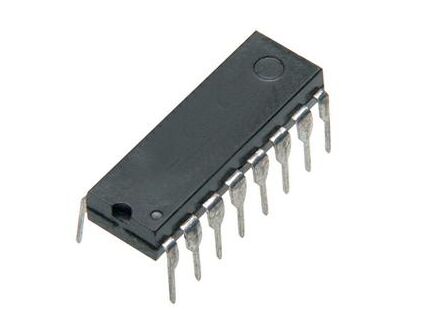
By Texas Instruments 183
CD4015 is an integrated circuit chip belonging to the CMOS logic series. It is a dual 4-bit static shift register with low power consumption, wide voltage operating range and good anti-interference performance. CD4015 integrates two independent 4-bit static shift registers, each register has one (Clock) and two data inputs (Serial Data A and Serial Data B). It can control the shifting and storing operations of data through the clock input.
The CD4015 is commonly used in data storage and shift register applications in digital logic circuits. CD4015 has two independent 4-bit memory units, each unit has a data input, a data output and control pins for reading, writing and shifting data.
Ⅰ.Specifications of CD4015
•Number of digits:4 bit
•Logic Series:40
•Number of pins:16
•Number of circuits:2
•Direction:One way
•Input capacitance:5 pF
•Number of input lines:1
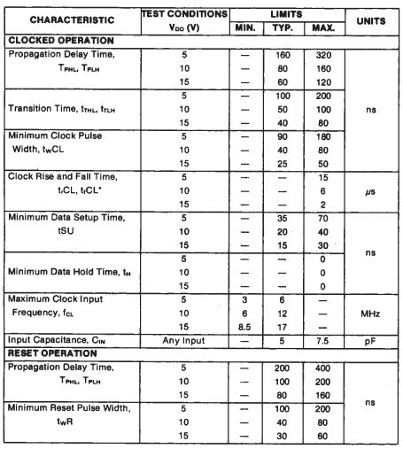
•Frequency:17MHz
•Output type:push-pull
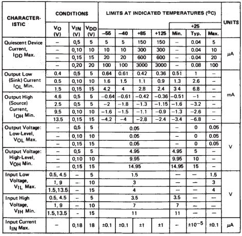
•Supply current:600 μA
•Logic type:CMOS
•Number of output lines:4
•Quiet current:100μA
•Terminal location:Dual
•Trigger type:Positive edge
•Power dissipation:500 mW
•Supply voltage-Maximum:18 V
•Minimum operating temperature:-55℃
•Maximum operating temperature:+125℃
•Function:Dual 4 Stage Static
•Installation style:Through Hole
•Counting order:Serial to Parallel
•Operating power supply voltage:500 mV to 20 V
•Product Category:Counter Shift Register
•Propagation delay time:320ns, 160ns, 120ns
Ⅱ.Working principle of CD4015
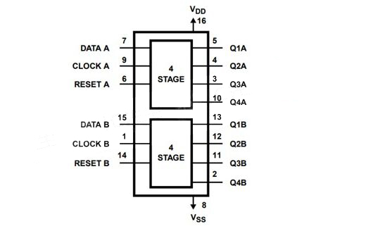
1.Memory unit: CD4015 has two independent 4-bit memory units, each unit contains four storage units (bits) for storing binary data. Each memory cell (bit) has an input and an output. Controlled by a clock signal, data can be transmitted and stored between the input and output terminals. On the rising or falling edge of the clock signal, data is transferred from the input to the output and can remain in the memory cell until the next clock signal arrives.
2.Parallel output: The stored data can be read in parallel through the parallel output (Q1, Q2, Q3, Q4 or ~Q1, ~Q2, ~Q3, ~Q4) pins.
3.Data input: Data can be input into the memory cell through the serial input (SER) pin. The input to a memory cell can be entered not only through the serial input, but also through the parallel input (A, B, C, D) pins simultaneously.
4.Control pins: CD4015 has some control pins, the main ones are the clock (CLK) and data storage (DS) pins.
•Clock pin (CLK): synchronizes data storage and read operations through a clock signal.
•Data storage pin (DS): When DS is high level, data storage is allowed to the memory unit; when DS is low level, data storage is prohibited.
5.Shift operation: Through the clock signal, CD4015 can realize the shift operation of data between memory cells. On the arrival of each clock pulse, data in a memory cell can move to adjacent memory cells. This shifting operation makes the CD4015 very flexible and useful in digital circuits. For example, through continuous shift operations, a data sequence can be moved from one memory unit to another memory unit to realize data transmission and caching.
Ⅲ.Main applications of CD4015
1.Shift register: The capabilities of CD4015 make it widely used in shift register circuits. Through the clock signal, it can realize the shifting of data between memory cells for rolling or delay operation of data.
2.Measurement system: CD4015 can be used in various measurement systems, such as time measurement, phase measurement, etc. By inputting the signal to the input terminal of CD4015, the processed signal can be obtained at the output terminal, thereby achieving signal measurement and analysis. In terms of time measurement, CD4015 can achieve signal delay through continuous shifting operations to obtain the time delay or period of the signal. By measuring the time difference between the CD4015's output signal and the clock signal, the time delay or period of the input signal can be obtained.
3.Control logic: In digital logic circuits, CD4015 can be used to store and control signals, such as timing control signals or status flags. By connecting the output of the CD4015 to the inputs of other digital logic gate circuits, various control logic functions can be implemented. By connecting the outputs of the CD4015 to the inputs of other digital logic gates, various control logic functions can be implemented.
4.Digital signal processing: CD4015 can be used in the field of digital signal processing, such as filtering, spectrum analysis, etc. Through shifting operations, signal processing such as delay, sampling, and interpolation can be implemented to improve signal quality or extract useful information. In terms of filtering, CD4015 can delay the signal through continuous shifting operations to build a simple delay filter. In terms of spectrum analysis, CD4015 can achieve signal sampling and interpolation through shifting operations. By controlling the frequency and number of sampling points of the clock signal, the discrete Fourier transform (DFT) or fast Fourier transform (FFT) can be performed on the input signal to obtain the spectrum information of the signal.
5.Counters and dividers: CD4015 can be used to build various counters and dividers. Through continuous shift operations, digital addition and subtraction counting and frequency division functions can be realized. This is useful for clock synchronization, frequency measurements, etc. In terms of counters, CD4015 can be used to implement binary counters or up and down counters. Through successive shift operations, the count value can be increased or decreased bit by bit. In terms of frequency dividers, CD4015 can also be used to implement various frequency divider circuits. Through continuous shifting operations, the frequency of the input signal can be lowered or raised.
6.Sequence/State Memory: The CD4015 can be used to store different states or sequences of the system as it provides multiple memory cells. In communication systems or control systems, CD4015 can be used to save a series of status information. This status information can be the amplitude, frequency, phase of the signal, or the status flag of a specific operation, etc. By reading the storage unit of CD4015, the current status of the system can be obtained at any time.
7.Parallel-to-serial data conversion: Since CD4015 supports parallel input and serial output, it can be used to convert parallel data to serial data, or vice versa. In practical applications, CD4015 can be used to implement data communications, serial bus interfaces, etc. For example, when data from a parallel processor needs to be transmitted to a serial communication line, the CD4015 can be used to convert the parallel data into serial data.
8.Clock frequency divider: With appropriate circuit configuration, the CD4015 can be used as a clock frequency divider to reduce the frequency of the input clock signal to the output clock signal. In the frequency divider circuit, after the input terminal of the CD4015 receives the clock signal, the data is shifted between the memory cells. By controlling the number of shifts, the frequency of the output clock signal can be changed. Specifically, if the CD4015 is configured to output a signal every N clock cycles, then the frequency of the output clock signal will be 1/N of the frequency of the input clock signal.
9.Analog switch control: By using multiple CD4015s, analog switch control can be achieved for selecting or routing different signal paths. By controlling the clock signal and data input of CD4015, different signal paths can be selected to implement signal routing and switching functions. This analog switch matrix can be used to implement complex signal processing and control systems, such as audio processing, radar systems, communication systems, etc.
Ⅳ.Characteristics of CD4015
•Serial Input and Parallel Output: One of the key features of the CD4015 is its dual-port design for serial input and parallel output. This allows it to process and transmit data simultaneously, improving data processing speed and efficiency.
•Replacement and equivalent shift register: CD4015 is a replacement or equivalent of 74HC595, CD4035, CD4014, CD4022 and other shift registers.
•Clock frequency: The CD4015 operates from a voltage range of 3V to 18V and operates at medium speed while consuming a low power consumption of 80uA. At an operating voltage of 15V, its clock frequency can reach 8.5Mhz.
•Power consumption and performance: CD4015 has low power consumption and stable performance, and is suitable for various application scenarios with high power consumption and performance requirements.
•Application scope: CD4015 is widely used in digital logic circuits, microprocessors, communication systems, clock generation, spectrum analysis, digital signal processing and other fields.
Ⅴ.Static Electrical Characteristics of CD4015
Ⅵ.Dynamic Electrical Characteristics f CD4015
Ⅶ.Steps to build electronic circuits using CD4015
1.Prepare materials:
•Cables, breadboards, etc.
•Appropriate power supply
•CD4015 chip
•Other required logic components (such as clock generators, gates, etc.)
2.Connect the power supply:
•Connect power to the CD4015, making sure the voltage meets chip specifications. Typically, the CD4015 operates in the 3V to 15V range.
3.Connect the clock signal:
•Connect the output of the clock generator to the clock pin (CLK) of the CD4015.
4.Connect data input:
•Determine whether to use serial or parallel input.
•If using parallel input, connect the parallel input pins (A, B, C, D) to the data source.
•If using serial input, connect the serial input pin (SER) to the data source.
5.Connect data storage control:
•Determines when data is allowed to be stored to the CD4015.
•Connect the data storage pin (DS) to a logic gate or other control circuit.
6.Connect other logic components:
•Need to connect other logic components, such as gate circuits, counters, timing controllers, etc.
7.Connect parallel output:
•If you need to read data in parallel, connect the parallel output pins (Q1, Q2, Q3, Q4) to other circuits.
8.Clock control:
•Adjust clock frequency and clock signal to meet the requirements of a specific application.
9.Testing and Debugging:
•Connect the circuit to a power source and observe the output of the CD4015 using test equipment or an oscilloscope.
•Adjust clock frequency, data input and other control parameters as needed to ensure proper circuit operation.
Ⅷ.Replacement model for CD4015
•MC14015B
•CD4015BE
•CD4015BEG4
•CD4015BF3A
•74HC4015
•HCF4015B
•CD74HC4015
Frequently Asked Questions
1.What is the CD4051?
The CD4051 is a CMOS analog multiplexer/demultiplexer integrated circuit. It allows for the selection of one of eight analog signals or one of eight digital signals under the control of three binary address lines.
2.How is the CD4051 controlled?
The CD4051 is controlled by three address lines (A, B, and C) that determine which input/output channel is active. The selection of the channel is based on the binary value represented by these three lines.
3.How many channels does the CD4051 have?
The CD4051 has 8 channels, which means it can handle 8 different analog or digital inputs.