By Adesto Technologies 181
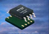
Adesto Technologies' AT45DBxxx DataFlash devices offer uniform page erase size as small as 256 bytes. This provides the user with the ability to perform completely self-contained, read-modify-write operations with minimal system overhead and management. The devices feature a common, but extensive, command interface and an 8-pin compatible footprint for easy migration from 1 Mbit to 64 Mbit densities. The Adesto programmed unique ID number, user-programmable sector protection, permanent sector locking, page erase capability, and integrated, fully independent SRAM buffers. This enables utilization of a single, very low pin-count memory device for all nonvolatile memory needs in terms of data storage, code shadow, or combined applications.
Current 2.5 V and 2.7 V minimum voltage options, as well as 1.65 V and 2.3 V minimum versions, are in development, but DataFlash devices align well with current futureASIC and SoC technologies. The DataFlash family provides flexibility, performance, ease-of-use, and can help drive your system cost reduction initiatives.
| Features | ||
|
|
New Products:
AT45DB161E-SHD-BAT45DB161E-SHD-TAT45DB161E-SSHD-BAT45DB161E-SSHD-TAT45DB021E-SSHN-TAT45DB041E-SSHN-TAT45DB041E-SSHN2B-TAT45DB041E-SHN-TAT45DB081E-SSHN-TAT45DB081E-SHN-BAT45DB161E-MHF-TAT45DB081E-SSHN-BAT45DB321E-SHF-TAT45DB321E-SHF2B-TAT45DB321E-MHF-TAT45DB321E-SHF-BAT45DB641E-MWHN-YAT45DB081E-SHN-TAT45DB021E-SHN-BAT45DB041E-SHN-B