By ON Semiconductor 56

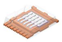
ON Semiconductor's innovative TO-LL technology offers an extremely low package resistance, a very small footprint, and allows for exceptionally good EMI behavior. This technology is now offered in a range of voltage classes specifically designed and qualified for automotive applications.
The combination of ON Semiconductor's latest PowerTrench shielded gate trench technology with the TO-LL package gives ON Semiconductor's leadless MOSFET products their extremely low RDS(ON) ranges. Both the superior silicon technology, as well as the package design, result in excellent switching and EMI performance, which is particularly beneficial for switching and PWM controlled applications in particular and has been verified by early customers of the devices. At the same time, it simplifies design, avoids additional passive components, and overall enables electronic manufacturers to better serve the markets for high-current applications. Compared to other discrete packages, the number of parallel MOSFETs needed in high-current applications can be significantly reduced, if not eliminated, leading to overall lower system costs.
Features and Benefits