By Littelfuse Inc 461

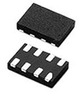
Littelfuse's SPA family of TVS diode array devices are designed to protect electronics from very fast and often damaging voltage transients, such as lightning and electrostatic discharge (ESD). They offer an ideal protection solution for analog and digital I/O interfaces for markets including consumer, telecommunications, industrial, medical, computing, and more.
ESD is an electrical transient that poses a serious threat to electronic circuits. The most common cause is friction between two dissimilar materials, causing a buildup of electric charges on their surfaces. Typically, one of the surfaces is the human body and it is not uncommon for this static charge to reach a potential as high as 15,000 volts. At 6,000 static volts, an ESD event will be painful to a person. Lower voltage discharges may go unnoticed, but can still cause catastrophic damage to electronic components and circuits. These robust diodes can safely absorb repetitive ESD strikes at the maximum level (Level 4) specified in the IEC 61000-4-2 international standard without performance degradation.
| Features | ||||
|
Microsite Link: SPA Family of TVS Diodes Arrays PTM Link: TVS Diode Arrays - ESD Suppressors for I/O Interfaces Littelfuse TVS Diode Array(PDF Format) (eBook Format) |