By Texas Instruments 25

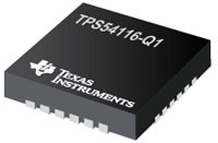
Texas Instruments' TPS54116-Q1 device is a full-featured, 6 V, 4 A, synchronous step-down converter with two integrated MOSFETs and a 1 A, sink/source, double date rate (DDR) VTT termination regulator with a VTTREF buffered reference output. The TPS54116-Q1 buck regulator minimizes solution size by integrating the MOSFETs and reducing inductor size with up to a 2.5 MHz switching frequency. The switching frequency can be set above the medium wave radio band for noise-sensitive applications and is synchronizable to an external clock. Synchronous rectification keeps the frequency fixed across the entire output load range. Efficiency is maximized through integrated, 25 mΩ low-side and 33 mΩ high-side MOSFETs. A cycle-by-cycle peak current limit protects the device during an over-current condition and is adjustable with a resistor at the ILIM pin to optimize it for smaller inductors.
The VTT termination regulator maintains fast transient response with only 2 x 10 µF ceramic output capacitance, reducing the external component count. The TPS54116-Q1 uses remote sensing of VTT for best regulation. Using the enable pins to enter a shutdown mode reduces supply current to 1 µA. Under-voltage lockout thresholds can be set with a resistor network on either enable pin. The VTT and VTTREF outputs are discharged when disabled with ENLDO. Full integration minimizes the IC footprint with a small, 4 mm x 4 mm, thermally enhanced WQFN package.
| Features | ||
|
|