By Toshiba Semiconductor and Storage 88
Toshiba introduces the next generation of super junction (SJ) deep trench semiconductor technology for high-efficient power MOSFETs. Devices based on the new DTMOS V process operate with lower EMI noise and reduced on resistance (RDS(ON)) compared to previous DTMOS IV MOSFETs.
As with the previous DTMOS IV semiconductor technology, DTMOS V is based on a single epitaxial process involving 'deep trench etching' followed by P-type epitaxial growth. The deep trench filling process results in a narrowing of cell pitch and a lowering of RDS(ON) when compared with more conventional planar processes. Toshiba's deep trench process allows an improved thermal coefficient of RDS(ON) compared to conventional super junction MOSFETs using multi-epitaxial growth process.
With DTMOS V, Toshiba has been able to reduce RDS(ON) of the DPAK TK290P60Y by up to 17% compared with the lowest RDS(ON) available from the TK12P60W DTMOS IV MOSFET. The company has also further optimized the trade-off between switching performance and EMI noise.
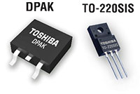
DTMOS V MOSFETs simplify the design and improve the performance of power conversion applications, including switching power supplies, power factor correction (PFC) designs, LED lighting, and other AC/DC applications. The first MOSFETs based on the fifth-generation process offer ratings of 600 V and 650 V and are supplied in DPAK (TO-252) and TO-220SIS (smart isolation) packaging. Maximum ON resistance ratings range from just 0.29 Ω to 0.56 Ω.