By Analog Devices Inc 27
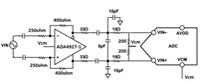
Analog Devices and LTC’s LTC2185 is a 16-bit, 2-channel simultaneously sampling analog-to-digital converter (ADC). With very low power consumption of 185 mW per channel from a single 1.8 V supply. This ADC has several output options such as CMOS, DDR CMOS, or DDR LVDS. The devices have a temperature range of 0°C to +70°C and come in a 64-pin QFN (9 mm x 9 mm) package. The LTC2185 is a great choice for cellular base stations, software defined radios (SDR), and medical imaging applications.
ADI’s ADA4927 is the ideal current feedback amplifier for high performance analog-to-digital converters like LTC’s LTC2185 part family. This amp is high speed (-3 dB bandwidth of 2.3 GHz), has extremely low harmonic distortion (-87 dBc HD2 at 100 MHz), and low input voltage noise at 1.4 nV/√Hz. The device has a temperature range of -40°C to +105°C and comes in a very small 3 mm x 3 mm LFCSP package. The ADA4927 is perfect for ADC driver, differential buffers, and IF and baseband gain blocks applications.
| LTC2185 Features | ADA4927 Features | |
|
|
|
| LTC2185 Applications | ADA4927 Applications | |
|
|