ADC32RF45 Dual-Channel ADC

By Texas Instruments 84
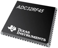
ADC32RF45 Dual-Channel ADC

Texas Instruments' ADC32RF45 device is a 14-bit, 3 GSPS, dual-channel, analog-to-digital converter (ADC) that supports RF sampling with input frequencies up to 4 GHz and beyond. Designed for high signal-to-noise ratio (SNR), the ADC32RF45 delivers a noise spectral density of -155 dBFS/Hz as well as dynamic range and channel isolation over a large input frequency range. The buffered analog input with on-chip termination provides uniform input impedance across a wide frequency range and minimizes sample-and-hold glitch energy.

Each ADC channel can be connected to a dual-band, digital down-converter (DDC) with up to three independent, 16-bit numerically controlled oscillators (NCOs) per DDC for phase-coherent frequency hopping. Additionally, the ADC is equipped with front-end peak and RMS power detectors and alarm functions to support external automatic gain control (AGC) algorithms.

The ADC32RF45 supports the JESD204B serial interface with subclass 1-based deterministic latency using data rates up to 12.5 Gbps with up to four lanes per ADC. The device is offered in a 72-pin VQFN package (10 mm x 10 mm) and supports the industrial temperature range (-40°C to +85°C).

TI Design Link: Efficient, LDO-Less, Power-Supply Network Reference Design for RF-Sampling ADC

Features
  • 14-bit, dual-channel, 3 GSPS ADC
  • Noise floor: -155 dBFS/Hz
  • RF input supports up to 4 GHz
  • Aperture jitter: 90 fS
  • Channel isolation: 95 dB at fIN = 1.8 GHz
  • Spectral performance (fIN = 900 MHz, -2 dBFS):
    • SNR: 60.9 dBFS
    • SFDR: 67 dBc HD2, HD3
    • SFDR: 77 dBc worst spur
  • Spectral performance (fIN = 1.78 GHz, -2 dBFS):
    • SNR: 58.8 dBFS
    • SFDR: 66 dBc HD2, HD3
    • SFDR: 75 dBc worst spur
  • On-chip input clamp for overvoltage protection
  • On-chip digital down-converters:
    • Up to four DDCs (dual-band mode)
    • Up to three independent NCOs per DDC
  • On-chip input clamp for overvoltage protection
  • Programmable on-chip power detectors with alarm pins for AGC support
  • On-chip dither
  • On-chip input termination
  • Input full-scale: 1.35 VPP
  • Support for multi-chip synchronization
  • JESD204B interface:
    • Subclass 1-based deterministic latency
    • Four lanes per channel at 12.5 Gbps
  • Power dissipation: 3.2 W/Ch at 3 GSPS
  • 72-pin VQFN package (10 mm x 10 mm) 
Applications
  • Multi-band, multi-mode 2G, 3G, 4G cellular receivers
  • Phased array radars
  • Electronic warfare
  • Cable infrastructure
  • Broadband wireless
  • High-speed digitizers
  • Software-defined radios
  • Communications test equipment
  • Microwave and millimeter wave receivers

Categories

Top