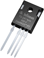
Infineon's vast portfolio of the 600 V CoolMOS P7 SJ MOSFET now includes an improved version of the standard TO-247 4-pin package. The TO-247 4-pin with asymmetric leads has 0.54 mm increased creepage distance between the critical leads which enables smoother wave soldering and reduced board yield loss. The additional connection to the source (Kelvin connection) that is used as a reference potential for the gate driving voltage eliminates the effect of voltage drops over the source inductance enabling faster switching transients which results in significant efficiency improvement. This allows for higher MOSFET RDS(on) usage and BOM cost savings. CoolMOS P7 is Infineon's best-balanced technology, with optimized balance of ease-of-use and highest energy efficiency.
The TO-247 4-pin concept (TO-247 vs. TO-247 4-pin)
|
|
|
|
|
|
|
- Re-turnon of MOSFET triggered by discharge of CGS
- Loss of efficiency
- Above simulation caused Eon losses of 130 µJ
|
|
- Clean waveform secured by 4th pin
- >2x reduction of turn-on losses
- Above simulation using TO-247 4-pin reduced losses by half Eon = 63 µJ
|
| Benefits |
|
Features |
- Suitable for hard and soft switching (PFC and LLC)
- Ease-of-use and fast design-in through low ringing tendency and usage across PFC and PWM stages
- Simplified thermal management due to low switching and conduction losses
- Higher manufacturing quality due to >2 kV ESD protection
- Increased power density solutions enabled by using products with a smaller footprint
- Suitable for a wide variety of applications and power ranges
- Reduced parasitic source inductance effects on the gate circuit enabling faster switching and increased efficiency
- Using benefits of Kelvin source efficiency allows usage of higher MOSFET RDS(on) and reduction of BOM cost
- Creepage distance meets 5,000 m altitude requirement
- Easier to design by customer
- Asymmetric leads enable simplified wave soldering and improved board yield loss
|
|
- Outstanding commutation ruggedness
- Optimized balance between efficiency and ease-of-use
- Significant reduction of switching and conduction losses
- Excellent ESD robustness >2 kV (HBM) for all products
- Better RDS(on) / package products compared to competition enabled by a low RDS(on) x A (below 1 Ω x mm2)
- Large portfolio with granular RDS(on) selection qualified for a variety of industrial and consumer grade applications
- 4th pin (Kelvin source)
- Increased creepage distance between high voltage pins
- Gate signal optimization
- Asymmetric leads increase critical pin distance
|
| Applications |
|
|
|
|
|
|