By Renesas 134
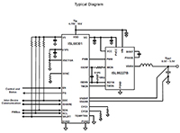
The ISL683xx family of products from Renesas Electronics America are single-out PWM controllers. These devices have integrated MOSFET drivers with PWM outputs that simplify designing power supplies for data center, wired and wireless communications, and factory automation equipment. The ISL68300 can drive discrete external MOSFETs directly, while the ISL68301 pairs with Renesas' smart power stages (SPS) or DrMOS power stages to create a complete voltage regulator solution. The ISL68301 is a PMBus compliant, single-phase digital DC/DC controller for use with SPS and DrMOS power stages. Both devices implement the Renesas fully digital ChargeMode™ control modulation scheme, allowing them to achieve both industry-leading performance and ease of use. ChargeMode control provides an inherently stable control loop that can respond to load transients in a single switching cycle, significantly decreasing output capacitor requirements. A dedicated current share bus allows for paralleling up to eight devices in a current share configuration, allowing support for a wide range of load currents. In conjunction with many other Renesas digital controllers, the ISL683xx family is capable of complex sequencing and fault spreading. The Digital-DC™ (DDC) bus is a single-wire serial bus which provides high-performance inter-device communication without the need for external sequencers, reducing overall system costs.
The PMBus interface facilitates device configuration, provides supply telemetry and detailed fault reporting including a parametric capture tool (SnapShot). These features are conveniently accessible through the PowerNavigator™ software tool. Additionally, a wide array of common configuration options are independently configurable through use of pin-strap resistors. The rich feature set in conjunction with the PowerNavigator software tool make the ISL683xx products ideal for telecom, servers, storage equipment, and power supply applications.
| Features | ||
|
|
|
| Applications | ||
|
|