LMK05028 Network Synchronizer Clock

By Texas Instruments 87
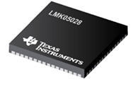
LMK05028 Network Synchronizer Clock

Texas Instruments' LMK05028 high-performance network synchronizer clock device provides jitter cleaning, clock generation, advanced clock monitoring, and superior hitless switching performance to meet the stringent timing requirements of communications infrastructure and industrial applications. The low-jitter and high-PSNR reduce bit error rates (BER) in high-speed serial links.

This device has two PLL channels and generates up to eight output clocks with 150 fs RMS jitter. Each PLL domain selects from any four reference inputs to synchronize its outputs.

Each PLL channel supports programmable loop bandwidth for jitter and wander attenuation and fractional frequency translation for flexible frequency configuration. Synchronization options supported on each PLL channel includes hitless switching with phase cancellation, digital holdover, DCO mode with < 1 ppt/step for precise clock steering (IEEE 1588 PTP slave), and zero-delay mode for deterministic input-to-output phase offset. The advanced reference input monitoring block ensures robust clock fault detection and helps to minimize output clock disturbance when a loss of reference (LOR) occurs.

This device uses a low-frequency TCXO/OCXO to determine the free-run or holdover frequency stability to maintain standards-compliant synchronization during LOR, or a standard XO when holdover frequency stability and wander are not critical. The LMK05028 is fully programmable through I2C or SPI interface and supports custom frequency configuration on power-up with the internal EEPROM or ROM. The EEPROM is factory pre-programmable and in-system programmable.

Features
  • Two independent PLL channels featuring:
    • Jitter: 150 fs RMS for outputs ≥ 100 MHz
    • Phase noise: -112 dBc/Hz at 100 Hz offset for 122.88 MHz
    • Hitless switching: 50 ps phase transient with phase cancellation
    • Programmable loop bandwidth with fastlock
    • Standards-compliant synchronization and holdover using a low-cost TCXO/OCXO
    • Any input to any output frequency translation
  • Four reference clock inputs
    • Priority-based input selection
    • Digital holdover on loss of reference
  • Industrial temperature range: -40°C to +85°C
  • Excellent power supply noise rejection (PSNR)
  • 3.3 V supply with 1.8 V, 2.5 V, or 3.3 V outputs
  • Eight clock outputs with programmable drivers
    • Up to six different output frequencies
    • AC-LVDS, AC-CML, AC-LVPECL, HCSL, and 1.8 V to 2.5 V LVCMOS output formats
  • EEPROM/ROM for custom clocks on power-up
  • Flexible configuration options
    • 1 Hz (1 PPS) to 750 MHz on input and output
    • XO: 10 MHz to 100 MHz, TCXO: 10 MHz to 54 MHz
    • DCO mode: < 1 ppt/step for fine frequency and phase-steering (IEEE 1588 slave)
    • Zero delay for deterministic phase-offset
    • Robust clock monitoring and status
    • I2C or SPI interface
Applications
  • SyncE (G.8262), SONET/SDH (Stratum 3/3E, G.813, GR-1244, GR-253), IEEE 1588 PTP slave clock, or optical transport network (G.709)
  • Telecom and enterprise line cards
  • Wireless base station (BTS), wireless backhaul
  • Test and measurements, broadcast infrastructures, and medical ultrasounds
  • Jitter and wander attenuation, precise frequency translation, and low-jitter clock generation for FPGA, DSP, ASIC, and CPU devices

Categories

Top