By NXP Semiconductors 99
Members of NXP's K32 L2 family are the latest members of NXP’s K32 L series. They are aimed at commercial and industrial IoT applications requiring an inexpensive, power-reserving MCU.
These MCUs feature a low-leakage architecture enabling multiple low-power modes. There are also low-power serial peripheral interfaces that support low-power operation modes that don’t require core activation.
NXP claims that the units require at least 54µA/MHz in very low power mode and less than 2uA in deep sleep mode.

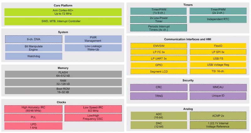
Block diagram for the K32 L2 MCU family. Image from NXP
Additionally, the devices offer security features such as a cyclic redundancy check, cryptographic acceleration technology, and a true random number generator.
CPU and Memory
The core processor is an Arm Cortex-M0+ core, which operates at speeds up to 48MHz. The processor also includes 32KB of RAM.
Non-volatile memory consists of:
Up to 256KB of program memory
A 16-byte flash configuration field that stores protection settings and security information
16KB ROM with a built-in bootloader to support the UART, I2C, USB, and SPI interfaces
The device includes a 32-byte system register file, which will be enabled in all power modes. A security circuitry is also in place to prevent unauthorized access to the RAM or flash from the debug port.
Power Management
A primary design goal that NXP has set for the (PDF) K32 L2 family is to use as little power as possible.
In the pursuit of that goal, the units’ power management controller (PMC) expands the operational modes of run, sleep, and deep sleep provided by Arm.
Within Arm’s Run operation mode, there are the run and very low power run (VLPR) configurations. Here, the MCU core is active and can access all the device’s many peripherals.
The difference between modes is the maximum clock frequency, which dictates power consumption.

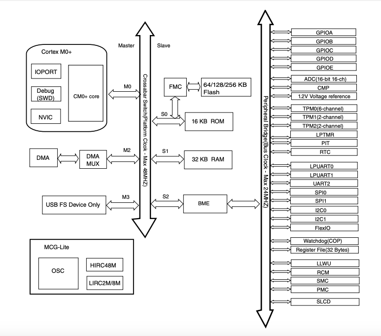
System diagram for members of the K32 l2B MCU family. Image from (PDF) NXP
The PMC provides its wait and very low power wait configurations within Arm’s sleep operation mode. Here, all of the peripherals can be enabled and operate as programmed, even though the MCU core is inactive.
The difference, again, is the maximum clock frequency of the system, which in turn affects power consumption.
Within Arm’s deep sleep operational mode, configurations include stop, very low power stop, low leakage stop, and very low leakage stop.
Here, the MCU core and most of the peripherals are off.
Security
Edge device security is a vital criterion for any IoT device. Once security is enabled, the serial wire debug port (SWD) can’t access the MCU’s memory. Also, the ROM boot loader can’t read out any information from the flash memory.
NXP explains that all members of the family feature a unique, factory-programmed 80-bit ID number.
Variations
There are 12 members of the K32 L2 family. In addition to the memory options already described, overall pin counts and GPIOs vary from 32 to 64 and 23 to 50, respectively.
The number of SE/DP ADC channels vary from 7/0 to 16/2. Six versions offer a segment LCD (SLCD) module to drive external LCD modules.

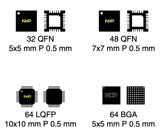
Packages for the members of the K32 L2 family. Image from (PDF) NXP
The varied units are available in 5mm x 5mm and 7mm x 7mm QFN packages, 5mm x 5mm MAPBGA packages, and 10mm x 10mm LQFP packages.
Evaluation and Support Tools
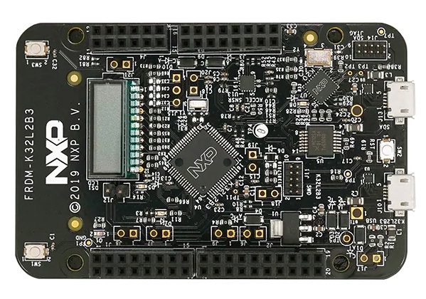
The FRDM-K32L2B3 freedom development board supports evaluation and development for members of the K32 L2B MCU family.

The FRDM-K32L2B3. Image from NXP
The board is fully supported by the MCUXpresso suite of tools. These include device drivers and middleware. NXP also provides examples to aid in rapid product development.