SN74SSQEC32882ZALR

SN74SSQEC32882ZALR
Mfr. #:
SN74SSQEC32882ZALR
Description:
Registers Low Pwr 28-56Bit Registered Buffer
Lifecycle:
New from this manufacturer.
Datasheet:
SN74SSQEC32882ZALR Datasheet
Delivery:
DHL FedEx Ups TNT EMS
Payment:
T/T Paypal Visa MoneyGram Western Union
ECAD Model:
More Information:
SN74SSQEC32882ZALR more Information SN74SSQEC32882ZALR Product Details
Product Attribute
Attribute Value
Manufacturer:
Texas Instruments
Product Category:
Registers
RoHS:
Y
Number of Circuits:
60
Maximum Clock Frequency:
945 MHz
Supply Voltage - Max:
+ 1.975 V
Supply Voltage - Min:
- 0.4 V
Minimum Operating Temperature:
0 C
Maximum Operating Temperature:
+ 85 C
Package / Case:
nFBGA-176
Packaging:
Reel
Series:
SN74SSQEC32882
Brand:
Texas Instruments
Mounting Style:
SMD/SMT
Moisture Sensitive:
Yes
Product Type:
Registers
Factory Pack Quantity:
2000
Subcategory:
Logic ICs
Unit Weight:
0.010935 oz
Tags
SN74SSQ, SN74SS, SN74S, SN74, SN7
Service Guarantees

We guarantee 100% customer satisfaction.

Quality Guarantees

We provide 90-360 days warranty.

If the items you received were not in perfect quality, we would be responsible for your refund or replacement, but the items must be returned in their original condition.
Our experienced sales team and tech support team back our services to satisfy all our customers.

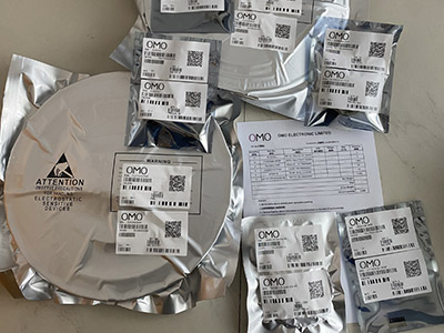
we buy and manage excess electronic components, including excess inventory identified for disposal.
Email us if you have excess stock to sell.

Email: info@omo-ic.com

Step1: Vacuum Packaging with PL
Step1:
Vacuum Packaging with PL
Step2: Anti-Static Bag
Step2:
Anti-Static Bag
Step3: Packaging Boxes
Step3:
Packaging Boxes
    A***a
    A***a
    CH

    Dishonest! He did not send the article but asks to wait! Never bought at Home

    2019-07-04
    V***h
    V***h
    RU

    Thank you seller the goods are excellent

    2019-02-07
    T***n
    T***n
    RO

    ok

    2019-01-30
***AS INSTRUMENTS INCORPORATED
This 1:2 or 26-bit 1:2 and 4-bit 1:1 registering clock driver with parity is designed for operation on DDR3 registered DIMMs with VDD of 1.5 V, on DDR3L registered DIMMs with VDD of 1.35 V and on DDR3U registered DIMMs with VDD of 1.25 V.
***AS INSTR
All inputs are 1.5 V, 1.35V and 1.25 V CMOS compatible. All outputs are CMOS drivers optimized to drive DRAM signals on terminated traces in DDR3 RDIMM applications. The clock outputs Yn and Yn and control net outputs DxCKEn, DxCSn and DxODTn can be driven with a different strength and skew to optimize signal integrity, compensate for different loading and equalize signal travel speed.
***AS
The SN74SSQEC32882 has two basic modes of operation associated with the Quad Chip Select Enable (QCSEN) input. When the QCSEN input pin is open (or pulled high), the component has two chip select inputs, DCS0 and DCS1, and two copies of each chip select output, QACS0, QACS1, QBCS0 and QBCS1. This is the "QuadCS disabled" mode. When the QCSEN input pin is pulled low, the component has four chip select inputs DCS[3:0], and four chip select outputs, QCS[3:0]. This is the "QuadCS enabled" mode. Through the remainder of this specification, DCS[n:0] will indicate all of the chip select inputs, where n=1 for QuadCS disabled, and n=3 for QuadCS enabled. QxCS[n:0] will indicate all of the chip select outputs.
***AS INSTRUM
The device also supports a mode where a single device can be mounted on the back side of a DIMM. If MIRROR=HIGH, Input Bus Termination (IBT) has to stay enabled for all input signals in this case.
***NS
The SN74SSQEC32882 operates from a differential clock (CK and CK). Data are registered at the crossing of CK going HIGH, and CK going LOW. This data could be either re-driven to the outputs or it could be used to access device internal control registers.
***AS INSTRUMENTS INCORPORATED
The input bus data integrity is protected by a parity function. All address and command input signals are added up and the last bit of the sum is compared to the parity signal delivered by the system at the input PAR_IN one clock cycle later. If they do not match the device pulls the open drain output ERROUT LOW. The control signals (DCKE0, DCKE1, DODT0, DODT1, DCS[n:0]) are not part of this computation.
***AS
The SN74SSQEC32882 implements different power saving mechanisms to reduce thermal power dissipation and to support system power down states. By disabling unused outputs the power consumption is further reduced.
***ASI
The package is optimized to support high density DIMMs. By aligning input and output positions towards DIMM finger signal ordering and SDRAM ballout the device de-scrambles the DIMM traces allowing low cross talk design with low interconnect latency.
***AS USD
Edge controlled outputs reduce ringing and improve signal eye opening at the SDRAM inputs.
Logic Solutions
OMO Electronic Logic Solutions offers a full spectrum of logic functions and technologies from the mature to the advanced, including bipolar, BiCMOS, and CMOS. TI's process technologies offer the logic performance and features required for modern logic designs, while maintaining support for more traditional logic products.Learn More
Part # Description Stock Price
SN74SSQEC32882ZALR
DISTI # 296-30095-1-ND
IC REGSTR BUFF 28-56BIT 176NFBGA
RoHS: Compliant
Min Qty: 1
Container: Cut Tape (CT)
1586In Stock
  • 1000:$4.7722
  • 500:$5.4792
  • 100:$6.2922
  • 10:$7.6000
  • 1:$8.4100
SN74SSQEC32882ZALR
DISTI # 296-30095-6-ND
IC REGSTR BUFF 28-56BIT 176NFBGA
RoHS: Compliant
Min Qty: 1
Container: Digi-Reel®
1586In Stock
  • 1000:$4.7722
  • 500:$5.4792
  • 100:$6.2922
  • 10:$7.6000
  • 1:$8.4100
SN74SSQEC32882ZALR
DISTI # 296-30095-2-ND
IC REGSTR BUFF 28-56BIT 176NFBGA
RoHS: Compliant
Min Qty: 2000
Container: Tape & Reel (TR)
Temporarily Out of Stock
  • 2000:$4.4616
SN74SSQEC32882ZALR
DISTI # SN74SSQEC32882ZALR
Registered Buffer Single 28-CH 176-Pin BGA T/R (Alt: SN74SSQEC32882ZALR)
RoHS: Compliant
Min Qty: 2000
Container: Tape and Reel
Asia - 0
    SN74SSQEC32882ZALR
    DISTI # SN74SSQEC32882ZALR
    Registered Buffer Single 28-CH 176-Pin BGA T/R - Tape and Reel (Alt: SN74SSQEC32882ZALR)
    RoHS: Compliant
    Min Qty: 2000
    Container: Reel
    Americas - 0
    • 2000:$4.8900
    • 4000:$4.6900
    • 8000:$4.4900
    • 12000:$4.3900
    • 20000:$4.2900
    SN74SSQEC32882ZALRJEDEC SSTE32882 Compliant Low Power 28-Bit to 56-Bit Registered Buffer with Address-Parity Test6000
    • 1000:$3.9000
    • 750:$3.9800
    • 500:$4.6000
    • 250:$5.2900
    • 100:$5.6600
    • 25:$6.3200
    • 10:$6.7600
    • 1:$7.5200
    SN74SSQEC32882ZALR
    DISTI # 595-74SSQEC32882ZALR
    Registers Low Pwr 28-56Bit Registered Buffer
    RoHS: Compliant
    0
    • 1:$8.1700
    • 10:$7.3800
    • 25:$6.8300
    • 100:$6.1100
    • 250:$5.8000
    • 500:$5.3200
    • 1000:$4.6400
    • 2000:$4.4700
    SN74SSQEC32882ZALRPLL Based Clock Driver, SSQE Series, 4 True Output(s), 0 Inverted Output(s), CMOS, PBGA176
    RoHS: Compliant
    18000
    • 1000:$4.5100
    • 500:$4.7500
    • 100:$4.9500
    • 25:$5.1600
    • 1:$5.5600
    Image Part # Description
    SN74SSQEB32882ZALR

    Mfr.#: SN74SSQEB32882ZALR

    OMO.#: OMO-SN74SSQEB32882ZALR

    Registers 28-56 Bit Registered Buffer
    SN74SSQEB32882ZALR

    Mfr.#: SN74SSQEB32882ZALR

    OMO.#: OMO-SN74SSQEB32882ZALR-TEXAS-INSTRUMENTS

    Registers 28-56 Bit Registered Buffe
    Availability
    Stock:
    Available
    On Order:
    1500
    Enter Quantity:
    Current price of SN74SSQEC32882ZALR is for reference only, if you want to get best price, please submit a inquiry or direct email to our sales team sales@omo-ic.com
    Reference price (USD)
    Quantity
    Unit Price
    Ext. Price
    1
    $8.17
    $8.17
    10
    $7.38
    $73.80
    25
    $6.83
    $170.75
    100
    $6.11
    $611.00
    250
    $5.80
    $1 450.00
    500
    $5.32
    $2 660.00
    1000
    $4.64
    $4 640.00
    Due to semiconductor in short supply from 2021,below price is the Normal price before 2021.please send inquire to confirm.
    Start with
    Newest Products
    Top