SN74V293-6PZA

SN74V293-6PZA
Mfr. #:
SN74V293-6PZA
Description:
FIFO 65536 x 18 Synch FIFO Memory
Lifecycle:
New from this manufacturer.
Datasheet:
SN74V293-6PZA Datasheet
Delivery:
DHL FedEx Ups TNT EMS
Payment:
T/T Paypal Visa MoneyGram Western Union
ECAD Model:
More Information:
SN74V293-6PZA more Information SN74V293-6PZA Product Details
Product Attribute
Attribute Value
Manufacturer:
Texas Instruments
Product Category:
FIFO
RoHS:
Y
Data Bus Width:
9 bit, 18 bit
Bus Direction:
Unidirectional
Memory Size:
1.125 Mbit
Timing Type:
Synchronous
Organization:
128 k x 9, 64 k x 18
Number of Circuits:
2
Maximum Clock Frequency:
166 MHz
Access Time:
4.5 ns
Supply Voltage - Max:
3.45 V
Supply Voltage - Min:
3.15 V
Supply Current - Max:
35 mA
Minimum Operating Temperature:
0 C
Maximum Operating Temperature:
+ 70 C
Package / Case:
LQFP-80
Packaging:
Tray
Height:
1.4 mm
Series:
SN74V293
Width:
14 mm
Brand:
Texas Instruments
Mounting Style:
SMD/SMT
Moisture Sensitive:
Yes
Operating Supply Voltage:
3.3 V
Product Type:
FIFO
Factory Pack Quantity:
90
Subcategory:
Memory & Data Storage
Unit Weight:
0.022575 oz
Tags
SN74V29, SN74V2, SN74V, SN74, SN7
Service Guarantees

We guarantee 100% customer satisfaction.

Quality Guarantees

We provide 90-360 days warranty.

If the items you received were not in perfect quality, we would be responsible for your refund or replacement, but the items must be returned in their original condition.
Our experienced sales team and tech support team back our services to satisfy all our customers.

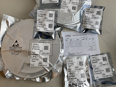
we buy and manage excess electronic components, including excess inventory identified for disposal.
Email us if you have excess stock to sell.

Email: info@omo-ic.com

Step1: Vacuum Packaging with PL
Step1:
Vacuum Packaging with PL
Step2: Anti-Static Bag
Step2:
Anti-Static Bag
Step3: Packaging Boxes
Step3:
Packaging Boxes
    Y***k
    Y***k
    RU

    Long delivery, already opened the dispute.

    2019-01-24
    H***l
    H***l
    DE

    great

    2019-04-25
    B***l
    B***l
    US

    Works perfectly.

    2019-05-30
***ow.cn
FIFO Mem Sync Dual Depth/Width Uni-Dir 64K x 18/128K x 9 80-Pin LQFP Tray
***as Instruments
65536 x 18 Synchronous FIFO Memory 80-LQFP 0 to 70
***AS
The SN74V263, SN74V273, SN74V283, and SN74V293 are exceptionally deep, high-speed, CMOS first-in first-out (FIFO) memories with clocked read and write controls and a flexible bus-matching ×9/×18 data flow.
***ASI
There is flexible ×9/×18 bus matching on both read and write ports.
***AS INTRUMENTS
The period required by the retransmit operation is fixed and short.
***AS INSRUMENTS
The first-word data-latency period, from the time the first word is written to an empty FIFO to the time it can be read, is fixed and short.
***TEXAS
These FIFOs are particularly appropriate for network, video, telecommunications, data communications, and other applications that need to buffer large amounts of data and match buses of unequal sizes.
***AS INST
Each FIFO has a data input port (Dn) and a data output port (Qn), both of which can assume either an 18-bit or 9-bit width, as determined by the state of external control pins’ input width (IW) and output width (OW) during the master-reset cycle.
***AS INS
The input port is controlled by write-clock (WCLK) and write-enable (WEN)\ inputs. Data is written into the FIFO on every rising edge of WCLK when WEN\ is asserted. The output port is controlled by read-clock (RCLK) and read-enable (REN)\ inputs. Data is read from the FIFO on every rising edge of RCLK when REN\ is asserted. An output-enable (OE)\ input is provided for 3-state control of the outputs.
***as Instr.
The frequencies of both the RCLK and the WCLK signals can vary from 0 to fMAX, with complete independence. There are no restrictions on the frequency of one clock input with respect to the other.
***AS INSRUMENTS
There are two possible timing modes of operation with these devices: first-word fall-through (FWFT) mode and standard mode.
***AS INSRUMENT
In FWFT mode, the first word written to an empty FIFO is clocked directly to the data output lines after three transitions of the RCLK signal. REN\ need not be asserted for accessing the first word. However, subsequent words written to the FIFO do require a low on REN\ for access. The state of the FWFT/SI input during master reset determines the timing mode in use.
***OMO Electronic
In standard mode, the first word written to an empty FIFO does not appear on the data output lines unless a specific read operation is performed. A read operation, which consists of activating REN\ and enabling a rising RCLK edge, shifts the word from internal memory to the data output lines.
***ASI
For applications requiring more data-storage capacity than a single FIFO can provide, the FWFT timing mode permits depth expansion by chaining FIFOs in series (i.e., the data outputs of one FIFO are connected to the corresponding data inputs of the next). No external logic is required.
***AS INSTR
These FIFOs have five flag pins: empty flag or output ready (EF\/OR\), full flag or input ready (FF\/IR\), half-full flag (HF)\, programmable almost-empty flag (PAE)\, and programmable almost-full flag (PAF)\. The IR\ and OR\ functions are selected in FWFT mode. The EF\ and FF\ functions are selected in standard mode. HF\, PAE\, and PAF\ always are available for use, regardless of timing mode.
***as Instruments Inc.
PAE\ and PAF\ can be programmed independently to switch at any point in memory. Programmable offsets determine the flag-switching threshold and can be loaded by parallel or serial methods. Eight default offset settings also are provided, so that PAE\ can be set to switch at a predefined number of locations from the empty boundary. The PAF\ threshold also can be set at similar predefined values from the full boundary. The default offset values are set during master reset by the state of FSEL0, FSEL1, and LD\.
***INS
For serial programming, SEN\, together with LD\, loads the offset registers via the serial input (SI) on each rising edge of WCLK. For parallel programming, WEN\, together with LD\, loads the offset registers via Dn on each rising edge of WCLK. REN\, together with LD\, can read the offsets in parallel from Qn on each rising edge of RCLK, regardless of whether serial or parallel offset loading has been selected.
***ASIN
Also, the timing modes of PAE\ and PAF\ outputs can be selected. Timing modes can be set to be either asynchronous or synchronous for PAE\ and PAF\.
***
If the asynchronous PAE\/PAF\ configuration is selected, PAE\ is asserted low on the low-to-high transition of RCLK. PAE\ is reset to high on the low-to-high transition of WCLK. Similarly, PAF\ is asserted low on the low-to-high transition of WCLK, and PAF\ is reset to high on the low-to-high transition of RCLK.
***AS INSTR
If the synchronous PAE\/PAF\ configuration is selected , PAE\ is asserted and updated on the rising edge of RCLK only and not WCLK. Similarly, PAF\ is asserted and updated on the rising edge of WCLK only and not RCLK. The desired mode is configured during master reset by the state of the programmable-flag mode (PFM) pin.
***AS INSTUMENTS
The retransmit function allows data to be reread from the FIFO more than once. A low on the RT\ input during a rising RCLK edge initiates a retransmit operation by setting the read pointer to the first location of the memory array. Zero-latency retransmit timing mode can be selected using the retransmit timing mode (RM). During master reset, a low on RM selects zero-latency retransmit. A high on RM during master reset selects normal latency.
***AS INSTRUMENTS INC
If zero-latency retransmit operation is selected, the first data word to be retransmitted is placed on the output register with respect to the same RCLK edge that initiated the retransmit, if RT\ is low.
***as Instruments Inc.
During master reset (MRS)\, the functions for all the operating modes are programmed. These include FWFT or standard timing, input bus width, output bus width, big endian or little endian, retransmit mode, programmable-flag operating and programming method, programmable-flag default offsets, and interspersed parity select. The read and write pointers are set to the first location of the FIFO. Then, based on the selected timing mode, EF\ is set low or OR\ is set high and FF\ is set high or IR\ is set low. Also, PAE\ is set low, PAF\ is set high, and HF\ is set high. The Q outputs are set low.
***TEXAS
Partial reset (PRS)\ also sets the read and write pointers to the first location of the memory. However, the timing mode, programmable-flag programming method, default or programmed offset settings, input and output bus widths, big endian/little endian, interspersed parity select, and retransmit mode existing before partial reset is asserted remain unchanged. The flags are updated according to the timing mode and offsets in effect. PRS\ is useful for resetting a device in mid-operation when reprogramming programmable flags and other functions would be undesirable.
***
A big-endian/little-endian data word format is provided. This function is useful when data is written into the FIFO in long-word (×18) format and read out of the FIFO in small-word (×9) format. If big-endian mode is selected, the most significant byte (MSB) (word) of the long word written into the FIFO is read out of the FIFO first, followed by the least significant byte (LSB). If little-endian format is selected, the LSB of the long word written into the FIFO is read out first, followed by the MSB. The mode desired is configured during master reset by the state of the big-endian/little-endian (BE)\ pin.
***as Instruments Inc.
The interspersed/noninterspersed parity (IP) bit function allows the user to select the parity bit in the word loaded into the parallel port (D0–Dn) when programming the flag offsets. If interspersed-parity mode is selected, the FIFO assumes that the parity bit is located in bit position D8 during the parallel programming of the flag offsets. If noninterspersed-parity mode is selected, D8 is assumed to be a valid bit and D16 and D17 are ignored. IP mode is selected during master reset by the state of the IP input pin. This mode is relevant only when the input width is set to ×18 mode.
***
The SN74V263, SN74V273, SN74V283, and SN74V293 are fabricated using TI’s high-speed submicron CMOS technology.
***AS INSTRUM
For more information on this device family, see the following application reports:
Part # Description Stock Price
SN74V293-6PZA
DISTI # V39:1801_07360562
FIFO Mem Sync Dual Depth/Width Uni-Dir 64K x 18/128K x 9 80-Pin LQFP Tray
RoHS: Compliant
33
  • 250:$32.9200
  • 100:$33.8300
  • 25:$37.5800
  • 10:$39.2100
  • 1:$42.0000
SN74V293-6PZA
DISTI # 296-12491-ND
IC SYNC FIFO MEM 65536X18 80LQFP
RoHS: Compliant
Min Qty: 1
Container: Tray
3338In Stock
  • 180:$35.8640
  • 90:$39.5741
  • 10:$41.3050
  • 1:$44.2700
SN74V293-6PZA
DISTI # 29459533
FIFO Mem Sync Dual Depth/Width Uni-Dir 64K x 18/128K x 9 80-Pin LQFP Tray
RoHS: Compliant
5400
  • 450:$37.3131
SN74V293-6PZA
DISTI # 26752180
FIFO Mem Sync Dual Depth/Width Uni-Dir 64K x 18/128K x 9 80-Pin LQFP Tray
RoHS: Compliant
33
  • 250:$35.3890
  • 100:$36.3672
  • 25:$40.3985
  • 10:$42.1508
  • 1:$45.1500
SN74V293-6PZA
DISTI # SN74V293-6PZA
FIFO Mem Sync Dual Depth/Width Uni-Dir 64K x 18/128K x 9 80-Pin LQFP - Trays (Alt: SN74V293-6PZA)
RoHS: Not Compliant
Min Qty: 90
Container: Tray
Americas - 0
  • 900:$28.2900
  • 540:$28.9900
  • 360:$29.7900
  • 180:$30.4900
  • 90:$30.8900
SN74V293-6PZA
DISTI # SN74V293-6PZA
FIFO Mem Sync Dual Depth/Width Uni-Dir 64K x 18/128K x 9 80-Pin LQFP (Alt: SN74V293-6PZA)
RoHS: Compliant
Min Qty: 90
Europe - 0
  • 900:€28.5900
  • 540:€29.7900
  • 360:€31.0900
  • 180:€34.0900
  • 90:€37.7900
SN74V293-6PZA65536 x 18 Synchronous FIFO Memory3600
  • 1000:$26.7700
  • 750:$26.8500
  • 500:$29.9200
  • 250:$31.8000
  • 100:$32.0400
  • 25:$36.0400
  • 10:$37.2200
  • 1:$39.8100
SN74V293-6PZA
DISTI # 595-SN74V293-6PZA
FIFO 65536 x 18 Synch FIFO Memory
RoHS: Compliant
85
  • 1:$42.1600
  • 5:$41.2300
  • 10:$39.3400
  • 25:$37.6900
  • 100:$34.1600
SN74V293-6PZAFIFO, 64KX18, 4.5ns, Synchronous, CMOS, PQFP80
RoHS: Compliant
1431
  • 1000:$31.0000
  • 500:$32.6300
  • 100:$33.9700
  • 25:$35.4300
  • 1:$38.1500
SN74V293-6PZA
DISTI # 6625374P
FIFO MEM SYNC DUAL DEPTH/WIDTH UNI-DIR, PU86
  • 5:£29.7200
Image Part # Description
TPS3801L30DCKR

Mfr.#: TPS3801L30DCKR

OMO.#: OMO-TPS3801L30DCKR

Supervisory Circuits 2.64V
MAX3232CPWR

Mfr.#: MAX3232CPWR

OMO.#: OMO-MAX3232CPWR

RS-232 Interface IC 3-5.5V Mult-Ch RS232
SN74LVC1G125DCKR

Mfr.#: SN74LVC1G125DCKR

OMO.#: OMO-SN74LVC1G125DCKR

Buffers & Line Drivers SINGLE BUS BUFFER GATE
MSP430F1232IRHBR

Mfr.#: MSP430F1232IRHBR

OMO.#: OMO-MSP430F1232IRHBR

16-bit Microcontrollers - MCU 8kB Flash 256B RAM 10bit ADC + 1 USART
L78M05CDT-TR

Mfr.#: L78M05CDT-TR

OMO.#: OMO-L78M05CDT-TR

Linear Voltage Regulators 5.0V 0.5A Positive
TPS61087DRCR

Mfr.#: TPS61087DRCR

OMO.#: OMO-TPS61087DRCR

Switching Voltage Regulators 650kHz/1.2MHz Step Up DC-DC Converter
LM2678S-ADJ/NOPB

Mfr.#: LM2678S-ADJ/NOPB

OMO.#: OMO-LM2678S-ADJ-NOPB

Switching Voltage Regulators HIGH EFF 5A STEP- DOWN VLTG REG
MCP1804T-3302I/DB

Mfr.#: MCP1804T-3302I/DB

OMO.#: OMO-MCP1804T-3302I-DB

LDO Voltage Regulators 150mA LDO Vin 28V Vout =3.3V
TLV2217-33KVURG3

Mfr.#: TLV2217-33KVURG3

OMO.#: OMO-TLV2217-33KVURG3

LDO Voltage Regulators Sgl Output LDO 500mA Fixed(3.3V)
LMV341IDBVR

Mfr.#: LMV341IDBVR

OMO.#: OMO-LMV341IDBVR

Operational Amplifiers - Op Amps Single Rail-To-Rail Output CMOS
Availability
Stock:
84
On Order:
2067
Enter Quantity:
Current price of SN74V293-6PZA is for reference only, if you want to get best price, please submit a inquiry or direct email to our sales team sales@omo-ic.com
Reference price (USD)
Quantity
Unit Price
Ext. Price
1
$42.16
$42.16
5
$41.23
$206.15
10
$39.34
$393.40
25
$37.69
$942.25
100
$34.16
$3 416.00
250
$32.98
$8 245.00
Due to semiconductor in short supply from 2021,below price is the Normal price before 2021.please send inquire to confirm.
Start with
Newest Products
Top