TC642
DS21444D-page 14 2001-2012 Microchip Technology Inc.
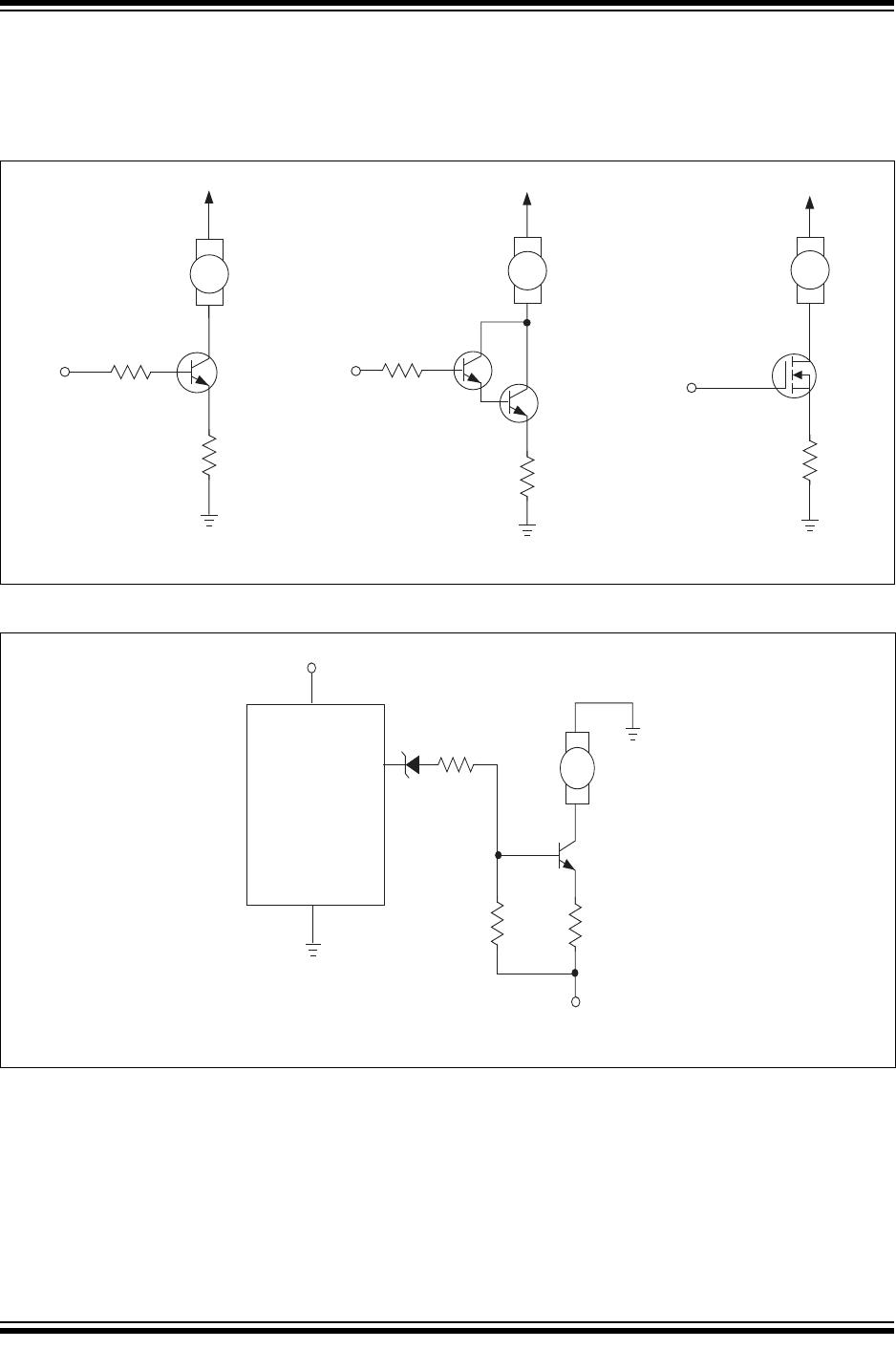
TABLE 5-2: TRANSISTORS AND MOSFETS FOR Q
1
(V
DD
= 5V)
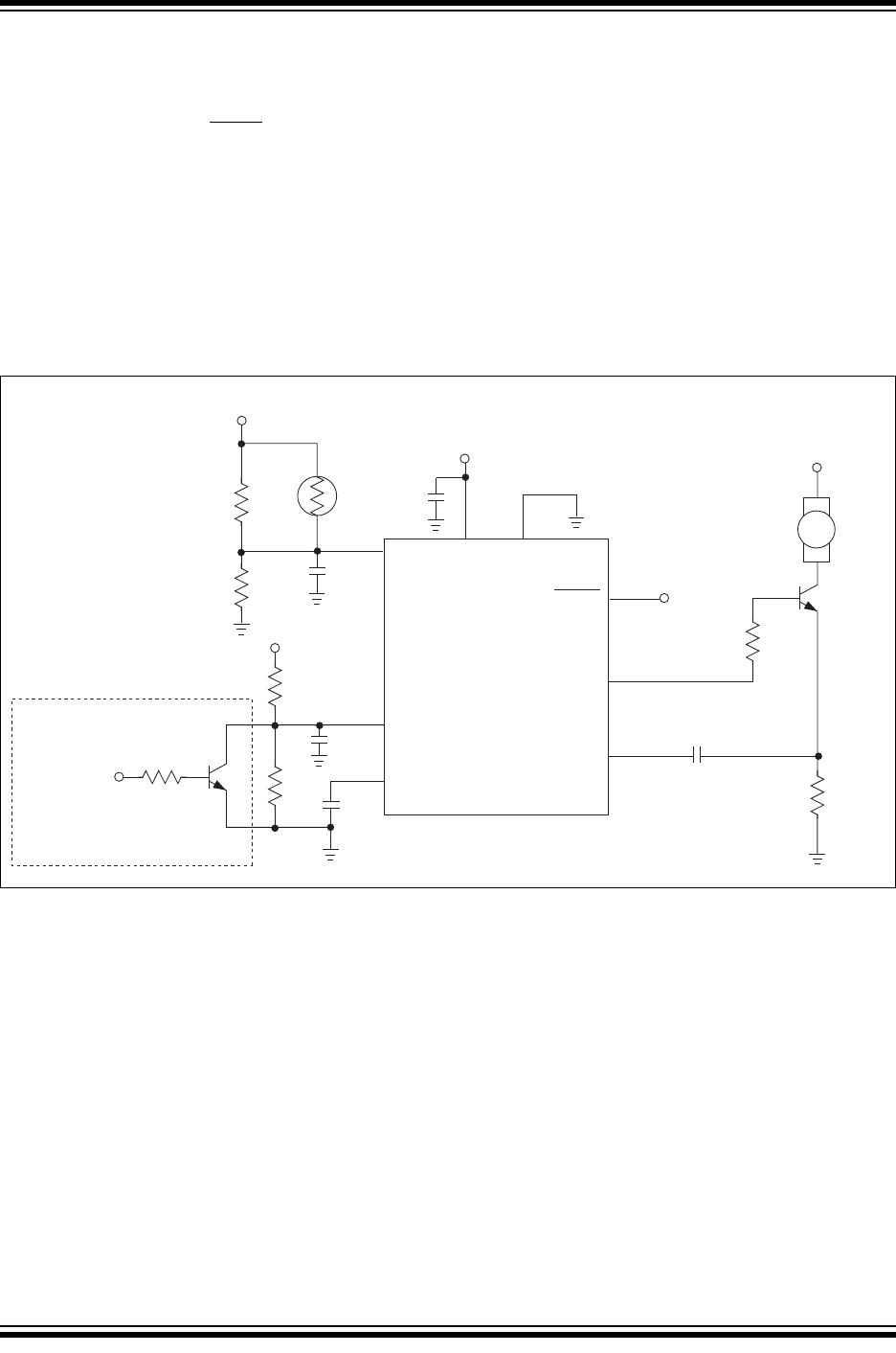
5.6 Latch-up Considerations
As with any CMOS IC, the potential exists for latch-up
if signals are applied to the device which are outside
the power supply range. This is of particular concern
during power-up if the external circuitry (such as the
sensor network, V
MIN
divider or shutdown circuit) is
powered by a supply different from that of the TC642.
Care should be taken to ensure that the TC642’s V
DD
supply powers up first. If possible, the networks
attached to V
IN
and V
MIN
should connect to the V
DD
supply at the same physical location as the IC itself.
Even if the IC and any external networks are powered
by the same supply, physical separation of the
connecting points can result in enough parasitic
capacitance and/or inductance in the power supply
connections to delay one power supply “routing” versus
another.
Device Package
Max. V
BE(sat)
/V
GS
(V)
Min. H
FE
V
CEO
/V
DS
(V)
Fan Current
(mA)
Suggested
R
BASE
()
MMBT2222A SOT-23 1.2 50 40 150 800
MPS2222A TO-92 1.2 50 40 150 800
MPS6602 TO-92 1.2 50 40 500 301
SI2302 SOT-23 2.5 NA 20 500 Note 1
MGSF1N02E SOT-23 2.5 NA 20 500 Note 1
SI4410 SO-8 4.5 NA 30 1000 Note 1
SI2308 SOT-23 4.5 NA 60 500 Note 1
Note 1: A series gate resistor may be used in order to control the MOSFET turn-on and turn-off times.