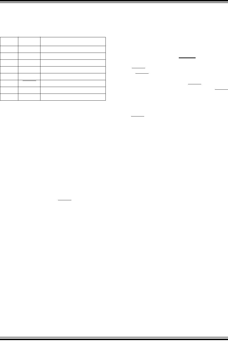
TC642
DS21444D-page 4 2001-2012 Microchip Technology Inc.
2.0 PIN DESCRIPTIONS
The descriptions of the pins are listed in Table 2-1.
TABLE 2-1: PIN FUNCTION TABLE
2.1 Analog Input (V
IN
)
The thermistor network (or other temperature sensor)
connects to the V
IN
input. A voltage range of 1.25V to
2.65V (typical) on this pin drives an active duty cycle of
0% to 100% on the V
OUT
pin.
2.2 Analog Output (C
F
)
C
F
is the positive terminal for the PWM ramp generator
timing capacitor. The recommended C
F
is 1 µF for
30 Hz PWM operation.
2.3 Analog Input (V
MIN
)
An external resistor divider connected to the V
MIN
input
sets the minimum fan speed by fixing the minimum
PWM duty cycle (1.25V to 2.65V = 0% to 100%, typi-
cal). The TC642 enters shutdown mode when V
MIN
V
SHDN
. During shutdown, the FAULT output is inactive
and supply current falls to 25 µA (typical). The TC642
exits shutdown mode when V
MIN
 V
REL
(see
Section 5.0, “Typical Applications”).
2.4 Ground (GND)
GND denotes the ground terminal.
2.5 Analog Input (SENSE)
Pulses are detected at the SENSE pin as fan rotation
chops the current through a sense resistor. The
absence of pulses indicates a fault.
2.6 Digital Output (FAULT)
The FAULT line goes low to indicate a fault condition.
When FAULT
goes low due to a fan fault condition, the
device is latched in shutdown mode until deliberately
cleared or until power is cycled. FAULT
may be con-
nected to V
MIN
if a hard shutdown is desired. FAULT
will also be asserted when the PWM reaches 100%
duty cycle, indicating that maximum cooling capability
has been reached and a possible over-temperature
condition may occur. This is a non-latching state and
the FAULT
output will go high when the PWM duty
cycle goes below 100%.
2.7 Digital Output (V
OUT
)
V
OUT
is an active high complimentary output that drives
the base of an external NPN transistor (via an appropri-
ate base resistor) or the gate of an N-channel MOS-
FET. This output has asymmetrical drive (see
Section 1.0, “Electrical Characteristics”).
2.8 Power Supply Input (V
DD
)
V
DD
may be independent of the fan’s power supply
(see Section 1.0, “Electrical Characteristics”).
Pin No. Symbol Description
1V
IN
Analog Input
2C
F
Analog Output
3V
MIN
Analog Input
4 GND Ground Terminal
5 SENSE Analog Input
6FAULT
Digital (Open Collector) Output
7V
OUT
Digital Output
8V
DD
Power Supply Input
2001-2012 Microchip Technology Inc. DS21444D-page 5
TC642
3.0 DETAILED DESCRIPTION
3.1 PWM
The PWM circuit consists of a ramp generator and
threshold detector. The frequency of the PWM is deter-
mined by the value of the capacitor connected to the C
F
input. A frequency of 30 Hz is recommended
(C
F
= 1 µF). The PWM is also the time base for the
Start-up Timer (see Section 3.4, “Start-Up Timer”). The
PWM voltage control range is 1.25V to 2.65V (typical)
for 0% to 100% output duty cycle.
3.2 FAULT Output
The TC642 detects faults in two ways.
First, pulses appearing at SENSE due to the PWM
turning on are blanked, with the remaining pulses
filtered by a missing pulse detector. If consecutive
pulses are not detected for 32 PWM cycles (1 Sec if
C
F
= 1 µF), the Diagnostic Timer is activated, and V
OUT
is driven high continuously for three PWM cycles
(100 msec if C
F
= 1 µF). If a pulse is not detected
within this window, the Start-up Timer is triggered (see
Section 3.4). This should clear a transient fault condi-
tion. If the missing pulse detector times out again, the
PWM is stopped and FAULT goes low. When FAULT is
activated due to this condition, the device is latched in
shutdown mode and will remain off indefinitely.
The TC642 may be configured to continuously attempt
fan restarts, if so desired.
Continuous restart mode is enabled by connecting the
FAULT
output to V
MIN
through a 0.01 µF capacitor, as
shown in Figure 3-1. When connected in this manner,
the TC642 automatically attempts to restart the fan
every time a fault condition occurs. When the FAULT
output is driven low, the V
MIN
input is momentarily
pulled below V
SHDN
, initiating a reset and clearing the
fault condition. Normal fan start-up is then attempted as
previously described. The FAULT
output may be
connected to external logic (or the interrupt input of a
microcontroller) to shut the TC642 down if multiple fault
pulses are detected at approximately one second
intervals. Diode D
1
, capacitor C
1
and resistors R
5
and
R
6
are provided to ensure fan restarts are the result of
a fan fault and not an over-temperature fault. A CMOS
logic OR gate may be substituted for these
components, if available.
FIGURE 3-1: Fan Fault Output Circuit.
Note: At this point, action must be taken to restart
the fan by momentarily pulling V
MIN
below
V
SHDN
, or cycling system power. In either
case, the fan cannot remain disabled due
to a fault condition, as severe system dam-
age could result. If the fan cannot be
restarted, the system should be shut down.
FAULT
SENSE
R
3
R
1
R
5
10kΩ
D
1
R
4
GND
From
System
Shutdown
Controller
(Optional)
*The parallel combination of R
3
and R
4
must be >10 kΩ.
Q
1
+12V
+5V
V
DD
V
IN
V
MIN
V
OUT
R
BASE
R
6
1kΩ
V
DD
R
SENSE
C
SENSE
C
F
1μF
C
F
TC642
Fan
C
B
0.01μF
1
8
6
7
5
4
2
3
From
Tem p
Sensor
+5V
0.01μF
1
0
TC642
RESET
Fault
Detected
C
1
Q
2
TC642
DS21444D-page 6 2001-2012 Microchip Technology Inc.
The second condition by which the TC642 detects a
fault is when the PWM control voltage applied to V
IN
becomes greater than that needed to drive 100% duty
cycle (see Section 1.0, “Electrical Characteristics”).
This indicates that the fan is at maximum drive and the
potential exists for system overheating. Either heat dis-
sipation in the system has gone beyond the cooling
system’s design limits or some subtle fault exists (such
as fan bearing failure or an airflow obstruction). This
output may be treated as a system overheat warning
and be used to trigger system shutdown. However, in
this case, the fan will continue to run even when FAULT
is asserted. If a shutdown is desired, FAULT may be
connected to V
MIN
outside the device. This will latch the
TC642 in shutdown mode when any fault occurs.
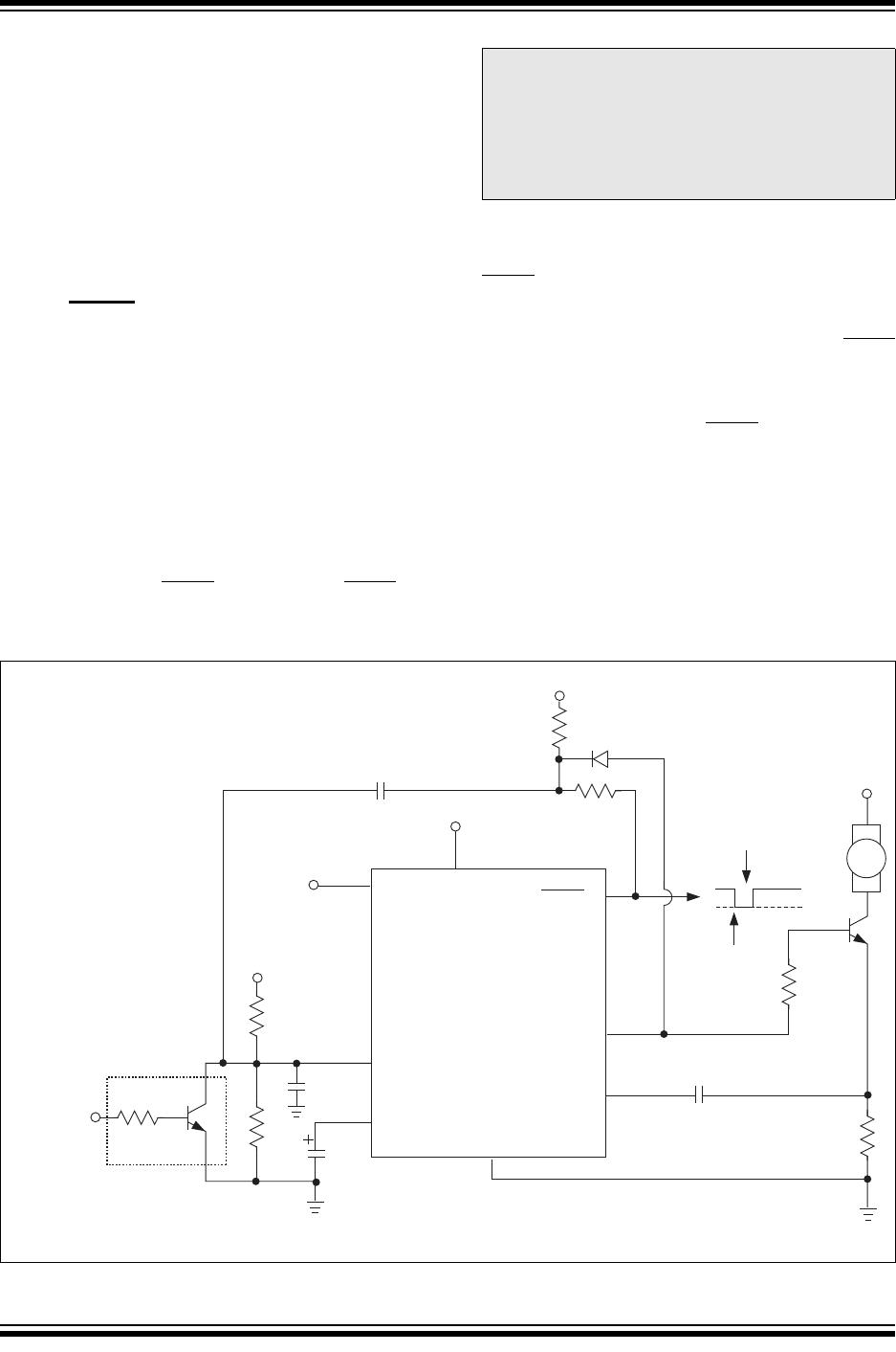
3.3 V
OUT
Output
The V
OUT
pin is designed to drive a low cost transistor
or MOSFET as the low side power switching element
in the system. Various examples of driver circuits will
be shown throughout this data sheet. This output has
asymmetric complementary drive and is optimized for
driving NPN transistors or N-channel MOSFETs. Since
the system relies on PWM rather than linear control,
the power dissipation in the power switch is kept to a
minimum. Generally, very small devices (TO-92 or
SOT packages) will suffice.
3.4 Start-Up Timer
To ensure reliable fan start-up, the Start-up Timer turns
the V
OUT
output on for 32 cycles of the PWM whenever
the fan is started from the off state. This occurs at
power-up and when coming out of shutdown mode. If
the PWM frequency is 30 Hz (C
F
= 1 µF), the resulting
start-up time will be approximately one second. If a
fault is detected, the Diagnostic Timer is triggered
once, followed by the Start-up Timer. If the fault per-
sists, the device is shut down (see Section 3.2, “FAULT
Output”).
3.5 Shutdown Control (Optional)
If V
MIN
(Pin 3) is pulled below V
SHDN
, the TC642 will go
into shutdown mode. This can be accomplished by
driving V
MIN
with an open-drain logic signal or by using
an external transistor, as shown in Figure 3-1. All func-
tions are suspended until the voltage on V
MIN
becomes
higher than V
REL
(0.85V @ V
DD
= 5.0V). Pulling V
MIN
below V
SHDN
will always result in complete device
shutdown and reset. The FAULT
output is
unconditionally inactive in shutdown mode.
A small amount of hysteresis, typically one percent of
V
DD
(50 mV at V
DD
= 5.0V), is designed into the V
SHDN
and
V
REL
thresholds. The levels specified for V
SHDN
and V
REL
in Section 1.0, “Electrical Characteristics”,
include this hysteresis, plus adequate margin to
account for normal variations in the absolute value of
the threshold and hysteresis.
3.6 SENSE Input
(FanSense
Technology)
The SENSE input (Pin 5) is connected to a low value
current sensing resistor in the ground return leg of the
fan circuit. During normal fan operation, commutation
occurs as each pole of the fan is energized. This
causes brief interruptions in the fan current, seen as
pulses across the sense resistor. If the device is not in
shutdown mode, and pulses are not appearing at the
SENSE input, a fault exists.
The short, rapid change in fan current (high dI/dt)
causes a corresponding dV/dt across the sense
resistor, R
SENSE
. The waveform on R
SENSE
is differen-
tiated and converted to a logic-level pulse-train by
C
SENSE
and the internal signal processing circuitry.
The presence and frequency of this pulse-train is a
direct indication of fan operation (see Section 5.0, “Typ-
ical Applications”, for more details).
CAUTION: Shutdown mode is unconditional. That is,
the fan will not be activated regardless of the voltage
at V
IN
. The fan should not be shut down until all heat
producing activity in the system is at a negligible level.

TC642CPA

Mfr. #:
Manufacturer:
Microchip Technology
Description:
Motor / Motion / Ignition Controllers & Drivers w/Fault Dtct
Lifecycle:
New from this manufacturer.
Delivery:
DHL FedEx Ups TNT EMS
Payment:
T/T Paypal Visa MoneyGram Western Union