2001-2012 Microchip Technology Inc. DS21444D-page 7
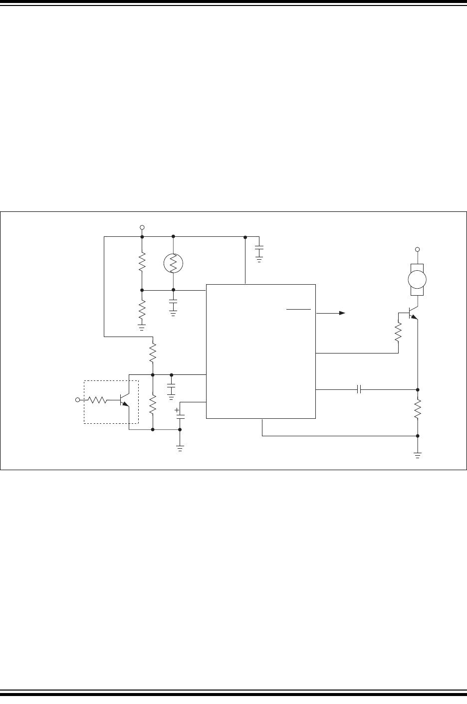
TC642
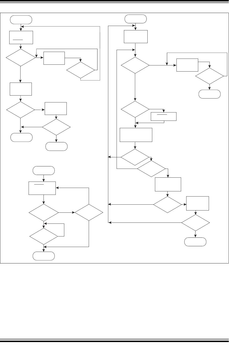
4.0 SYSTEM BEHAVIOR
The flowcharts describing the TC642’s behavioral
algorithm are shown in Figure 4-1. They can be
summarized as follows:
4.1 Power-Up
(1) Assuming the device is not being held in shutdown
mode (V
MIN
> V
REL
)…
(2) Turn V
OUT
output on for 32 cycles of the PWM
clock. This ensures that the fan will start from a
dead stop.
(3) During this Start-up Timer, if a fan pulse is
detected, branch to Normal Operation; if none are
received…
(4) Activate the 32-cycle Start-up Timer one more time
and look for a fan pulse; if a fan pulse is detected,
proceed to Normal Operation; if none are
received…
(5) Proceed to Fan Fault.
(6) End.
4.2 Normal Operation
Normal Operation is an endless loop which may only
be exited by entering shutdown mode or Fan Fault. The
loop can be thought of as executing at the frequency of
the oscillator and PWM.
(1) Reset the missing pulse detector.
(2) Is TC642 in shutdown? If so…
a. V
OUT
duty cycle goes to zero.
b. FAULT
is disabled.
c. Exit the loop and wait for V
MIN
> V
REL
to
resume operation (indistinguishable from
power-up).
(3) If an over-temperature fault occurs (V
IN
> V
OTF
),
activate FAULT
; release FAULT when V
IN
< V
OTF
.
(4) Drive V
OUT
to a duty cycle proportional to the
greater of V
IN
and V
MIN
on a cycle by cycle basis.
(5) If a fan pulse is detected, branch back to the start
of the loop (1).
(6) If the missing pulse detector times out …
(7) Activate the 3-cycle Diagnostic Timer and look for
pulses; if a fan pulse is detected, branch back to
the start of the loop (1); if none are received…
(8) Activate the 32-cycle Start-up Timer and look for
pulses; if a fan pulse is detected, branch back to
the start of the loop (1); if none are received…
(9) Quit Normal Operation and go to Fan Fault.
(10) End.
4.3 Fan Fault
Fan fault is an infinite loop wherein the TC642 is
latched in shutdown mode. This mode can only be
released by a reset (i.e., V
MIN
being brought below
V
SHDN
, then above V
REL
, or by power-cycling).
(1) While in this state, FAULT
is latched on (low) and
the V
OUT
output is disabled.
(2) A reset sequence applied to the V
MIN
pin will exit
the loop to Power-Up.
(3) End.