DS064 (v6.3) April 3, 2006 www.xilinx.com 1
Product Specification
© 1996-2006 Xilinx, Inc. All rights reserved. All Xilinx trademarks, registered trademarks, patents, and disclaimers are as listed at http://www.xilinx.com/legal.htm.
All other trademarks and registered trademarks are the property of their respective owners. All specifications are subject to change without notice.
Features
• 5 ns pin-to-pin logic delays on all pins
•f
CNT
to 100 MHz
• 36 macrocells with 800 usable gates
• Up to 34 user I/O pins
• 5V in-system programmable
- Endurance of 10,000 program/erase cycles
- Program/erase over full commercial voltage and
temperature range
• Enhanced pin-locking architecture
• Flexible 36V18 Function Block
- 90 product terms drive any or all of 18 macrocells
within Function Block
- Global and product term clocks, output enables,
set and reset signals
• Extensive IEEE Std 1149.1 boundary-scan (JTAG)
support
• Programmable power reduction mode in each
macrocell
• Slew rate control on individual outputs
• User programmable ground pin capability
• Extended pattern security features for design
protection
• High-drive 24 mA outputs
• 3.3V or 5V I/O capability
• Advanced CMOS 5V FastFLASH™ technology
• Supports parallel programming of more than one
XC9500 concurrently
• Available in 44-pin PLCC, 44-pin VQFP, 48-pin CSP
packages
Description
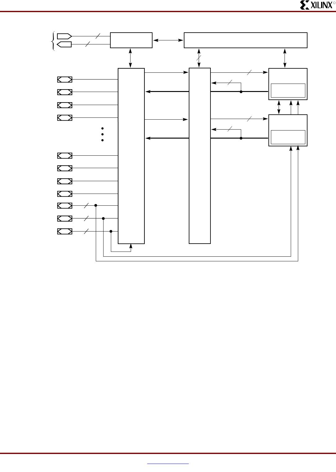
The XC9536 is a high-performance CPLD providing
advanced in-system programming and test capabilities for
general purpose logic integration. It is comprised of eight
36V18 Function Blocks, providing 800 usable gates with
propagation delays of 5 ns. See Figure 2 for the architecture
overview.
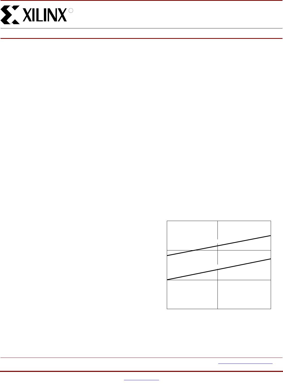
Power Management
Power dissipation can be reduced in the XC9536 by config-
uring macrocells to standard or low-power modes of opera-
tion. Unused macrocells are turned off to minimize power
dissipation.
Operating current for each design can be approximated for
specific operating conditions using the following equation:
I
CC
(mA) = MC
HP
(1.7) + MC
LP
(0.9) + MC (0.006 mA/MHz) f
Where:
MC
HP
= Macrocells in high-performance mode
MC
LP
= Macrocells in low-power mode
MC = Total number of macrocells used
f = Clock frequency (MHz)
Figure 1 shows a typical calculation for the XC9536 device.
0
XC9536 In-System
Programmable CPLD
DS064 (v6.3) April 3, 2006
05
Product Specification
R
Figure 1:
Typical I
CC
vs. Frequency for XC9536
Clock Frequency (MHz)
Typical I
CC
(mA)
050
(50)
(30)
(83)
(50)
100
High Performance
Low Power
DS064_01_110101