XC9536-10PC44C

XC9536 In-System Programmable CPLD
4 www.xilinx.com DS064 (v6.3) April 3, 2006
Product Specification
R
AC Characteristics
Symbol Parameter
XC9536-5 XC9536-6 XC9536-7 XC9536-10 XC9536-15
UnitsMin Max Min Max Min Max Min Max Min Max
T
PD
I/O to output valid - 5.0 - 6.0 - 7.5 - 10.0 - 15.0 ns
T
SU
I/O setup time before GCK 3.5 - 3.5 - 4.5 - 6.0 - 8.0 - ns
T
H
I/O hold time after GCK 0 - 0 - 0 - 0 - 0 - ns
T
CO
GCK to output valid - 4.0 - 4.0 - 4.5 - 6.0 - 8.0 ns
f
CNT
(1)
16-bit counter frequency 100.0 - 100.0 - 125.0 - 111.1 - 95.2 - MHz
f
SYSTEM
(2)
Multiple FB internal operating
frequency
100.0 - 100.0 - 83.3 - 66.7 - 55.6 - MHz
T
PSU
I/O setup time before p-term
clock input
0.5 - 0.5 - 0.5 - 2.0 - 4.0 - ns
T
PH
I/O hold time after p-term clock
input
3.0 - 3.0 - 4.0 - 4.0 - 4.0 - ns
T
PCO
P-term clock output valid - 7.0 - 7.0 - 8.5 - 10.0 - 12.0 ns
T
OE
GTS to output valid - 5.0 - 5.0 - 5.5 - 6.0 - 11.0 ns
T
OD
GTS to output disable - 5.0 - 5.0 - 5.5 - 6.0 - 11.0 ns
T
POE
Product term OE to output
enabled
- 9.0 - 9.0 - 9.5 - 10.0 - 14.0 ns
T
POD
Product term OE to output
disabled
- 9.0 - 9.0 - 9.5 - 10.0 - 14.0 ns
T
WLH
GCK pulse width (High or Low) 4.0 - 4.0 - 4.0 - 4.5 - 5.5 - ns
T
APRPW
Asynchronous preset/reset
pulse width (High or Low)
7.0 - 7.0 - 7.0 - 7.5 - 8.0 - ns
Notes:
1. f
CNT
is the fastest 16-bit counter frequency available, using the local feedback when applicable.
f
CNT
is also the Export Control Maximum flip-flop toggle rate, f
TOG
.
2. f
SYSTEM
is the internal operating frequency for general purpose system designs spanning multiple FBs.
Figure 3:
AC Load Circuit
Device Output
Output Type V
TEST
5.0V
3.3V
V
TEST
R
1
160Ω
260Ω
R
1
R
2
C
L
R
2
120Ω
360Ω
C
L
35 pF
35 pF
DS067_03_110101
V
CCIO
5.0V
3.3V
XC9536 In-System Programmable CPLD
DS064 (v6.3) April 3, 2006 www.xilinx.com 5
Product Specification
R
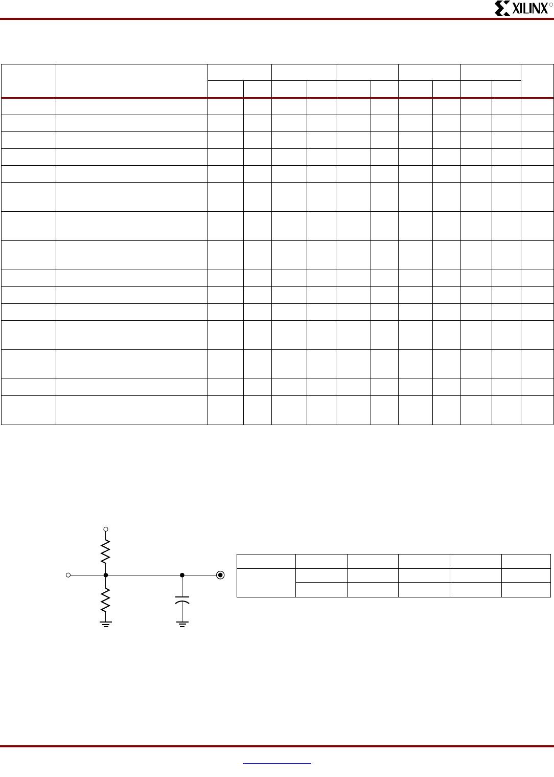
Internal Timing Parameters
Symbol Parameter
XC9536-5 XC9536-6 XC9536-7 XC9536-10 XC9536-15
UnitsMinMaxMinMaxMinMaxMinMaxMinMax
Buffer Delays
T
IN
Input buffer delay - 1.5 - 1.5 - 2.5 - 3.5 - 4.5 ns
T
GCK
GCK buffer delay - 1.5 - 1.5 - 1.5 - 2.5 - 3.0 ns
T
GSR
GSR buffer delay - 4.0 - 4.0 - 4.5 - 6.0 - 7.5 ns
T
GTS
GTS buffer delay - 5.0 - 5.0 - 5.5 - 6.0 - 11.0 ns
T
OUT
Output buffer delay - 2.0 - 2.0 - 2.5 - 3.0 - 4.5 ns
T
EN
Output buffer enable/disable delay - 0 - 0 - 0 - 0 - 0 ns
Product Term Control Delays
T
PTCK
Product term clock delay - 3.0 - 3.0 - 3.0 - 3.0 - 2.5 ns
T
PTSR
Product term set/reset delay - 1.0 - 1.0 - 2.0 - 2.5 - 3.0 ns
T
PTTS
Product term 3-state delay - 5.5 - 5.5 - 4.5 - 3.5 - 5.0 ns
Internal Register and Combinatorial Delays
T
PDI
Combinatorial logic propagation delay - 0.5 - 0.5 - 0.5 - 1.0 - 3.0 ns
T
SUI
Register setup time 2.5 - 2.5 - 1.5 - 2.5 - 3.5 - ns
T
HI
Register hold time 1.0 - 1.0 - 3.0 - 3.5 - 4.5 - ns
T
COI
Register clock to output valid time - 0.5 - 0.5 - 0.5 - 0.5 - 0.5 ns
T
AOI
Register async. S/R to output delay - 6.0 - 6.0 - 6.5 - 7.0 - 8.0 ns
T
RAI
Register async. S/R recover before
clock
5.0 - 5.0 - 7.5 - 10.0 - 10.0 - ns
T
LOGI
Internal logic delay - 1.0 - 1.0 - 2.0 - 2.5 - 3.0 ns
T
LOGILP
Internal low power logic delay - 9.0 - 9.0 - 10.0 - 11.0 - 11.5 ns
Feedback Delays
T
F
FastCONNECT feedback delay - 6.0 - 6.0 - 8.0 - 9.5 - 11.0 ns
Time Adders
T
PTA
(1)
Incremental product term allocator
delay
- 0.8 - 0.8 - 1.0 - 1.0 - 1.0 ns
T
SLEW
Slew-rate limited delay - 3.5 - 3.5 - 4.0 - 4.5 - 5.0 ns
Notes:
1. T
PTA
is multiplied by the span of the function as defined in the XC9500 family data sheet.
XC9536 In-System Programmable CPLD
6 www.xilinx.com DS064 (v6.3) April 3, 2006
Product Specification
R
XC9536 I/O Pins
XC9536 Global, JTAG and Power Pins
Function
Block
Macroce
ll
PC44 VQ44 CS48
BSca
n
Order
Function
Block
Macroce
ll
PC44 VQ44 CS48
BSca
n
Order
1 1 2 40 D6 105 2 1 1 39 D7 51
1 2 3 41 C7 102 2 2 44 38 E5 48
1 3 5
[1]
43
[1]
B7
[1]
99 2 3 42
[1]
36
[1]
E6
[1]
45
1 4 4 42 C6 96 2 4 43 37 E7 42
1 5 6
[1]
44
[1]
B6
[1]
93 2 5 40
[1]
34
[1]
F6
[1]
39
1 6 8 2A690 2 6 39
[1]
33
[1]
G7
[1]
36
1 7 7
[1]
1
[1]
A7
[1]
87 2 7 38 32 G6 33
1 8 9 3C584 2 8 3731F530
1 9 11 5B581 2 9 3630G527
1 10 12 6 A4 78 2 10 35 29 F4 24
1 11 13 7 B4 75 2 11 34 28 G4 21
1 12 14 8 A3 72 2 12 33 27 E3 18
1 13 18 12 B2 69 2 13 29 23 F2 15
1 14 19 13 B1 66 2 14 28 22 G1 12
1 15 20 14 C2 63 2 15 27 21 F1 9
1 16 22 16 C3 60 2 16 26 20 E2 6
1 17 24 18 D2 57 2 17 25 19 E1 3
118-54 218---0
Notes: :
1. Global control pin.
Pin Type PC44 VQ44 CS48
I/O/GCK1 5 43 B7
I/O/GCK2 6 44 B6
I/O/GCK3 7 1 A7
I/O/GTS1 42 36 E6
I/O/GTS2 40 34 F6
I/O/GSR 39 33 G7
TCK 17 11 A1
TDI 15 9 B3
TDO 30 24 G2
TMS 16 10 A2
V
CCINT
5V 21, 41 15, 35 C1,F7
V
CCIO
3.3V/5V 32 26 G3
GND 23, 10, 31 17, 4, 25 A5, D1, F3
No Connects C4, D3, D4, E4

XC9536-10PC44C

Mfr. #:
Manufacturer:
Xilinx
Description:
Lifecycle:
New from this manufacturer.
Delivery:
DHL FedEx Ups TNT EMS
Payment:
T/T Paypal Visa MoneyGram Western Union