©2014 Silicon Storage Technology, Inc. DS20005053B 04/14
14
4 Mbit (x16) Multi-Purpose Flash Plus
SST39VF401C / SST39VF402C / SST39LF401C / SST39LF402C
Data Sheet
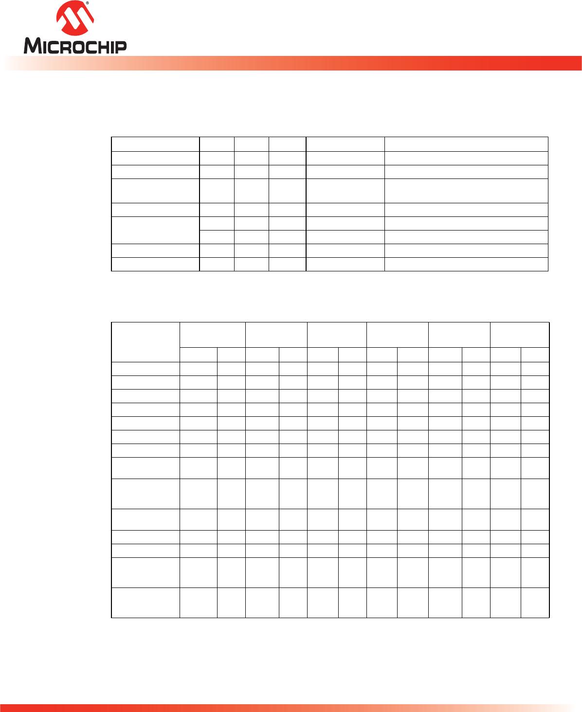
5. With A
MS
-A
4
= 0; Sec ID is read with A
3
-A
0
,
Microchip ID is read with A
3
= 0 (Address range = 000000H to 000007H),
User ID is read with A
3
= 1 (Address range = 000008H to 000087H).
Lock Status is read with A
7
-A
0
= 0000FFH. Unlocked: DQ
3
= 1 / Locked: DQ
3
=0.
6. Valid Word-Addresses for Sec ID are from 000000H-000007H and 000008H-000087H.
7. The device does not remain in Software Product ID Mode if powered down.
8. With A
MS
-A
1
=0; Microchip Manufacturer ID = 00BFH, is read with A
0
=0,
SST39VF401C/SST39LF401C Device ID = 233BH, is read with A
0
= 1, SST39VF402C/SST39LF402C Device ID =
233AH, is read with A
0
=1,
A
MS
= Most significant address; A
MS
=A
17
9. Both Software ID Exit operations are equivalent
10. If users never lock after programming, Sec ID can be programmed over the previously unprogrammed bits (data=1)
using the Sec ID mode again (the programmed ‘0’ bits cannot be reversed to ‘1’). Valid Word-Addresses for Sec ID are
from 000000H-000007H and 000008H-000087H.
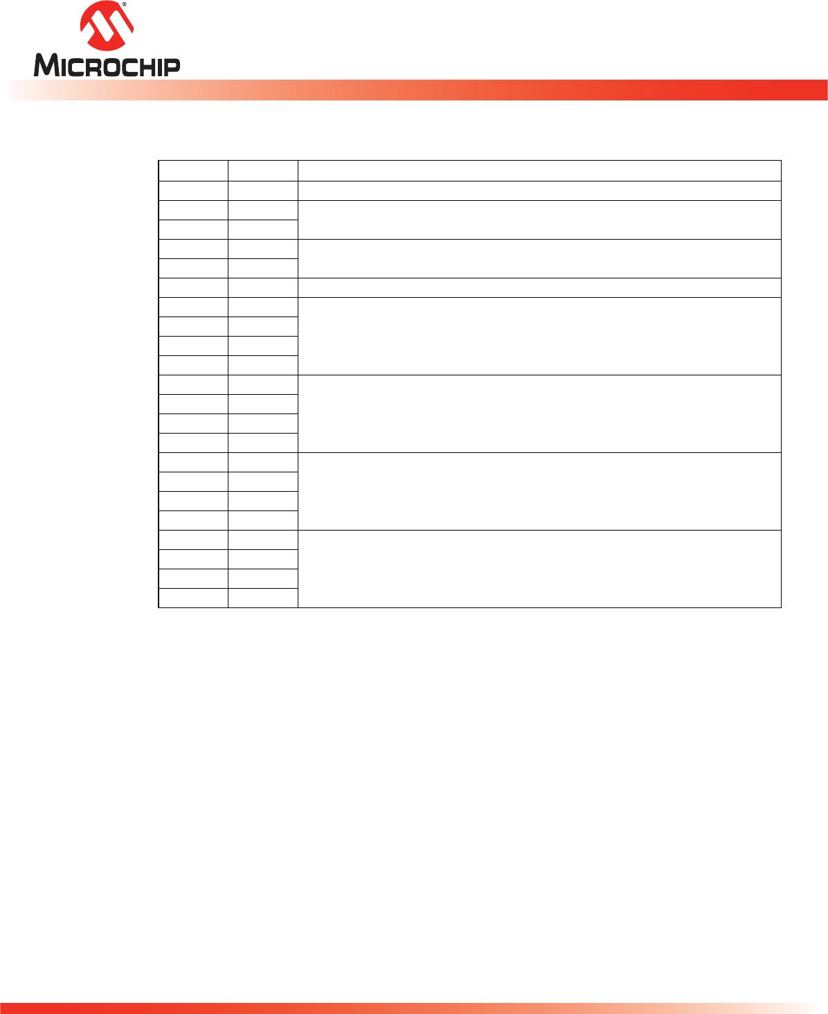
Table 8: CFI Query Identification String
1
Address Data Data
10H 0051H Query Unique ASCII string “QRY”
11H 0052H
12H 0059H
13H 0002H Primary OEM command set
14H 0000H
15H 0000H Address for Primary Extended Table
16H 0000H
17H 0000H Alternate OEM command set (00H = none exists)
18H 0000H
19H 0000H Address for Alternate OEM extended Table (00H = none exits)
1AH 0000H
T8.1 25053
1. Refer to CFI publication 100 for more details.
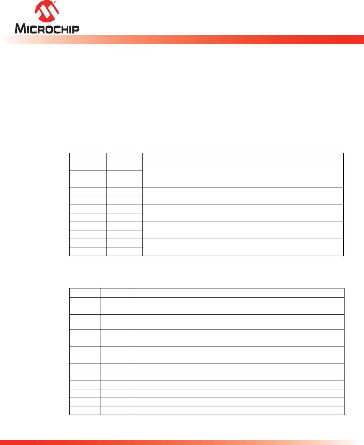
Table 9: System Interface Infor mation
Address Data Data
1BH 0027H V
DD
Min (Program/Erase)
DQ
7
-DQ
4
: Volts, DQ
3
-DQ
0
: 100 millivolts
1CH 0036H V
DD
Max (Program/Erase)
DQ
7
-DQ
4
: Volts, DQ
3
-DQ
0
: 100 millivolts
1DH 0000H V
PP
min. (00H = no V
PP
pin)
1EH 0000H V
PP
max. (00H = no V
PP
pin)
1FH 0003H Typical time out for Word-Program 2
N
µs (2
3
= 8 µs)
20H 0000H Typical time out for min. size buffer program 2
N
µs (00H = not supported)
21H 0004H Typical time out for individual Sector/Block-Erase 2
N
ms (2
4
=16ms)
22H 0005H Typical time out for Chip-Erase 2
N
ms (2
5
=32ms)
23H 0001H Maximum time out for Word-Program 2
N
times typical (2
1
x2
3
=16µs)
24H 0000H Maximum time out for buffer program 2
N
times typical
25H 0001H Maximum time out for individual Sector/Block-Erase 2
N
times typical (2
1
x2
4
=32ms)
26H 0001H Maximum time out for Chip-Erase 2
N
times typical (2
1
x2
5
=64ms)
T9.3 25053