©2014 Silicon Storage Technology, Inc. DS20005053B 04/14
16
4 Mbit (x16) Multi-Purpose Flash Plus
SST39VF401C / SST39VF402C / SST39LF401C / SST39LF402C
Data Sheet
Electrical Specifications
Absolute Maximum Stress Ratings (Applied conditions greater than those listed under “Absolute
Maximum Stress Ratings” may cause permanent damage to the device. This is a stress rating only and
functional operation of the device at these conditions or conditions greater than those defined in the
operational sections of this data sheet is not implied. Exposure to absolute maximum stress rating con-
ditions may affect device reliability.)
Temperature Under Bias .............................................. -55°C to +125°C
Storage Temperature ................................................ -65°C to +150°C
D. C. Voltage on Any Pin to Ground Potential .............................-0.5V to V
DD
+0.5V
Transient Voltage (<20 ns) on Any Pin to Ground Potential ..................-2.0V to V
DD
+2.0V
Voltage on A
9
Pin to Ground Potential .....................................-0.5V to 13.2V
Package Power Dissipation Capability (T
A
= 25°C) ................................... 1.0W
Surface Mount Solder Reflow ...................................... 260°C for 10 seconds
Output Short Circuit Current
1
.................................................. 50mA
1. Outputs shorted for no more than one second. No more than one output shorted at a time.
Table 11: Operating Range
Range Ambient Temp V
DD
Commercial 0°C to +70°C 2.7-3.6V for SST39VF401C/402C or
3.0-3.6V for SST39LF401C/402C
Industrial -40°C to +85°C 2.7-3.6V for SST39VF401C/402C or
3.0-3.6V for SST39LF401C/402C
T11.0 25053
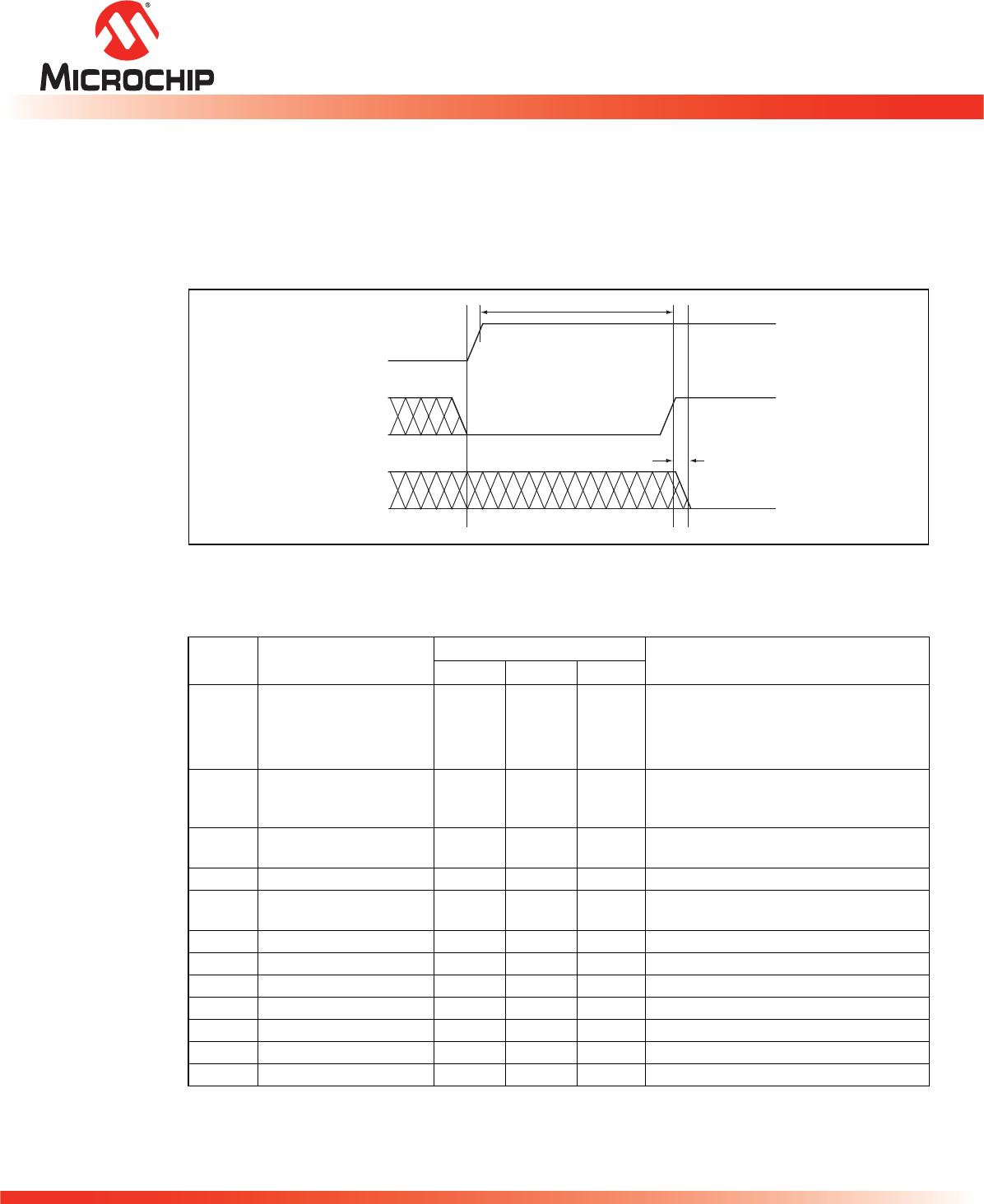
Table 12: AC Conditions of Test
1
1. See Figures 20 and 21
Input Rise/Fall Time Output Load
5ns C
L
=30pF
T12.1 25053
©2014 Silicon Storage Technology, Inc. DS20005053B 04/14
17
4 Mbit (x16) Multi-Purpose Flash Plus
SST39VF401C / SST39VF402C / SST39LF401C / SST39LF402C
Data Sheet
Power Up Specifications
All functionalities and DC specifications are specified for a V
DD
ramp rate of greater than 1V per 100
ms (0V to 3V in less than 300 ms). If the VDD ramp rate is slower than 1V per 100 ms, a hardware
reset is required. The recommended V
DD
power-up to RESET# high time should be greater than 100
µs to ensure a proper reset.
Figure 5: Power-Up Diagram
Table 13: DC Operating Characteristics V
DD
= 3.0-3.6V for SST39LF401C/402C and 2.7-
3.6V for SST39VF401C/402C
1
1. Typical conditions for the Active Current shown on the front page of the data sheet are average values at 25°C
(room temperature), and V
DD
= 3V. Not 100% tested.
Symbol Parameter
Limits
Test ConditionsMin Max Units
I
DD
Power Supply Current Address input=V
ILT
/V
IHT
2
, at f=5 MHz,
V
DD
=V
DD
Max
2. See Figure 20
Read
3
3. The I
DD
current listed is typically less than 2mA/MHz, with OE# at V
IH.
Typical V
DD
is 3V.
18 mA CE#=V
IL
, OE#=WE#=V
IH
, all I/Os open
Program and Erase 30 mA CE#=WE#=V
IL
, OE#=V
IH
I
SB
Standby V
DD
Current 20 µA CE#=V
IHC
,V
DD
=V
DD
Max
RST#=V
DD
±0.3, WP#=V
DD
±0.3,
WE#=V
DD
±0.3
I
ALP
Auto Low Power 20 µA CE#=V
ILC
,V
DD
=V
DD
Max
All inputs=V
SS
or V
DD,
WE#=V
IHC
I
LI
Input Leakage Current 1 µA V
IN
=GND to V
DD
,V
DD
=V
DD
Max
I
LIW
Input Leakage Current
on WP# pin and RST#
10 µA WP#=GND to V
DD
or RST#=GND to V
DD
I
LO
Output Leakage Current 10 µA V
OUT
=GND to V
DD
,V
DD
=V
DD
Max
V
IL
Input Low Voltage 0.8 V V
DD
=V
DD
Min
V
ILC
Input Low V oltage (CMOS) 0.3 V V
DD
=V
DD
Max
V
IH
Input High Voltage 0.7V
DD
V
DD
+0.3 V V
DD
=V
DD
Max
V
IHC
Input High V oltage (CMOS) V
DD
-0.3 V
DD
+0.3 V V
DD
=V
DD
Max
V
OL
Output Low Voltage 0.2 V I
OL
=100 µA, V
DD
=V
DD
Min
V
OH
Output High Voltage V
DD
-0.2 V I
OH
=-100 µA, V
DD
=V
DD
Min
T13.8 25053
25053 F24.0
V
DD
RESET#
CE#
T
PU-READ
10s
V
DD
min
0V
V
IH
T
RHR
5 0ns
©2014 Silicon Storage Technology, Inc. DS20005053B 04/14
18
4 Mbit (x16) Multi-Purpose Flash Plus
SST39VF401C / SST39VF402C / SST39LF401C / SST39LF402C
Data Sheet
Table 14: Recommended System Power-up Timings
Symbol Parameter Minimum Units
T
PU-READ
1
1. This parameter is measured only for initial qualification and after a design or process change that could affect this
parameter.
Power-up to Read Operation 100 µs
T
PU-WRITE
1
Power-up to Program/Erase Operation 100 µs
T14.0 25053
Table 15: Capacitance (T
A
= 25°C, f=1 Mhz, other pins open)
Parameter Description Test Condition Maximum
C
I/O
1
1. This parameter is measured only for initial qualification and after a design or process change that could affect this
parameter.
I/O Pin Capacitance V
I/O
=0V 12pF
C
IN
1
Input Capacitance V
IN
=0V 6pF
T15.0 25053
Table 16: Reliability Characteristics
Symbol Parameter Minimum Specification Units Test Method
N
END
1,2
1. This parameter is measured only for initial qualification and after a design or process change that could affect this
parameter.
2. N
END
endurance rating is qualified as a 10,000 cycle minimum for the whole device. A sector- or block-level rating would
result in a higher minimum specification.
Endurance 10,000 Cycles JEDEC Standard A117
T
DR
1
Data Retention 100 Years JEDEC Standard A103
I
LTH
1
Latch Up 100 + I
DD
mA JEDEC Standard 78
T16.2 25053

SST39VF401C-70-4I-EKE

Mfr. #:
Manufacturer:
Microchip Technology
Description:
NOR Flash 2.7 to 3.6V 4Mbit Multi-Purpose Flash
Lifecycle:
New from this manufacturer.
Delivery:
DHL FedEx Ups TNT EMS
Payment:
T/T Paypal Visa MoneyGram Western Union