© Semiconductor Components Industries, LLC, 2012
March, 2017 − Rev. 2
1 Publication Order Number:
MMBT2222AM3/D
MMBT2222AM3T5G
NPN General Purpose
Transistor
The MMBT2222AM3T5G device is a spin−off of our popular
SOT−23 three−leaded device. It is designed for general purpose
amplifier applications and is housed in the SOT−723 surface mount
package. This device is ideal for low−power surface mount
applications where board space is at a premium.
Features
• Reduces Board Space
• NSV Prefix for Automotive and Other Applications Requiring
Unique Site and Control Change Requirements; AEC−Q101
Qualified and PPAP Capable
• These Devices are Pb−Free, Halogen Free/BFR Free and are RoHS
Compliant
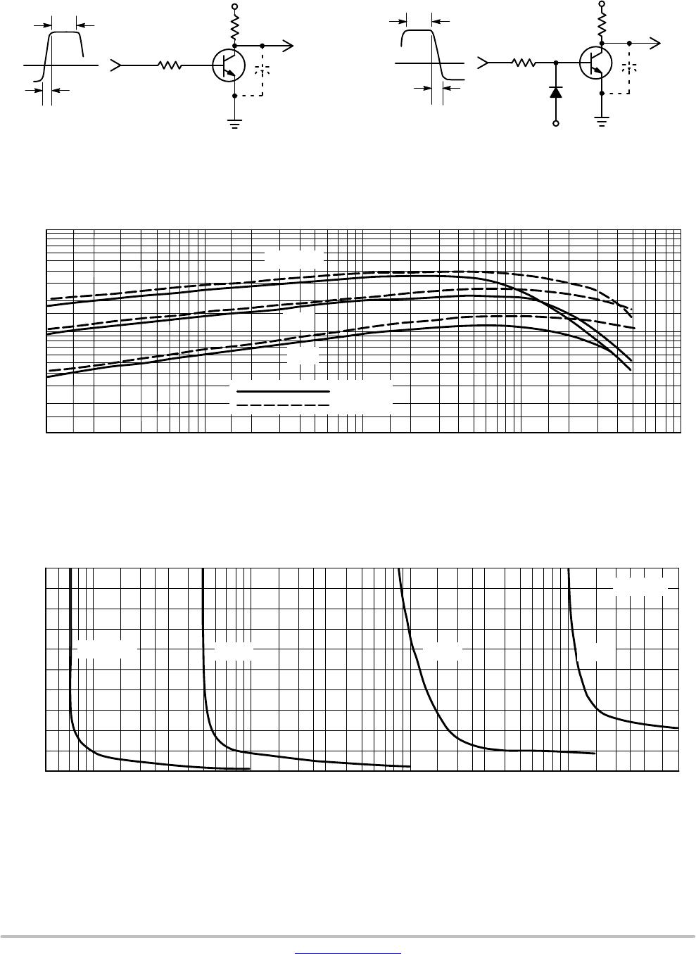
MAXIMUM RATINGS
Rating Symbol Value Unit
Collector−Emitter Voltage V
CEO
40 Vdc
Collector−Base Voltage V
CBO
75 Vdc
Emitter−Base Voltage V
EBO
6.0 Vdc
Collector Current − Continuous I
C
600 mAdc
THERMAL CHARACTERISTICS
Characteristic Symbol Max Unit
Total Device Dissipation
FR−5 Board (Note 1)
T
A
= 25°C
Derate above 25°C
P
D
265
2.1
mW
mW/°C
Thermal Resistance,
Junction−to−Ambient
R
q
JA
470 °C/W
Total Device Dissipation
Alumina Substrate, (Note 2) T
A
= 25°C
Derate above 25°C
P
D
640
5.1
mW
mW/°C
Thermal Resistance,
Junction−to−Ambient
R
q
JA
195 °C/W
Junction and Storage Temperature T
J
, T
stg
−55 to
+150
°C
Stresses exceeding those listed in the Maximum Ratings table may damage the
device. If any of these limits are exceeded, device functionality should not be
assumed, damage may occur and reliability may be affected.
1. FR−5 = 1.0 0.75 0.062 in.
2. Alumina = 0.4 0.3 0.024 in. 99.5% alumina.
www.onsemi.com
Device Package Shipping
†
ORDERING INFORMATION
MMBT2222AM3T5G SOT−723
(Pb−Free)
8000/Tape &
Reel
COLLECTOR
3
1
BASE
2
EMITTER
†For information on tape and reel specifications,
including part orientation and tape sizes, please
refer to our Tape and Reel Packaging Specifications
Brochure, BRD8011/D.
SOT−723
CASE 631AA
STYLE 1
1
2
3
AA M
AA = Specific Device Code
M = Date Code
MARKING
DIAGRAM
NSVMMBT2222AM3T5G SOT−723
(Pb−Free)
8000/Tape &
Reel