7
LT1684
BASIC THEORY OF OPERATION
The LT1684 operates using a user-provided pulse-width-
modulated (PWM) digital signal as input*. The low fre-
quency modulation component of this signal represents
the desired output waveform. Changing the PWM input
can thus dynamically control the frequency, cadence,
amplitude and DC offset of the desired output. This method
of sine wave generation can accomodate all popular ring
tone frequencies including 17Hz, 20Hz, 25Hz and 50Hz.
The LT1684 receives the PWM input by a capacitor-
isolated differential input at pins IN A and IN B. This signal
is amplitude normalized by a bandgap reference and
output single-ended on the BG
OUT
pin such that the PWM
carrier is ±1.25V about the voltage on the OUT pin.
The low frequency component of the normalized PWM
signal is recovered using an active filter circuit con-
structed using an onboard driver amplifier. This amplifier
also provides current drive for the final ring tone output.
The ring tone output is used as the reference for a floating
active biasing scheme by pin AT
REF
. As the ring tone
output rises and falls through its typical range of hundreds
of volts, the LT1684 “tracks” the output signal, maintain-
ing local supply voltages across the IC of approximately
±10V.
Input Receiver/Reference Buffer
The differential receiver for the PWM input signal requires
minimum differential input levels of 1.6V to assure valid
change-of-state. The receiver inputs are capacitor coupled,
isolating the LT1684 from the PWM generator. The re-
ceiver is leading edge triggered.
The input receiver controls a switched-state output that
forces an amplitude normalized voltage (referenced to the
OUT pin) of ±1.25V that follows the PWM input. This
switched voltage is driven off-chip on pin BG
OUT
. When
the IN A input is driven higher than IN B (by the required
1.6V), the reference drives BG
OUT
to +1.25V above OUT.
When IN B input is driven higher than IN A, BG
OUT
is forced
to –1.25V relative to OUT.
The amplitude normalized representation of the input
PWM signal is used as the input for the active filter element
and output driver.
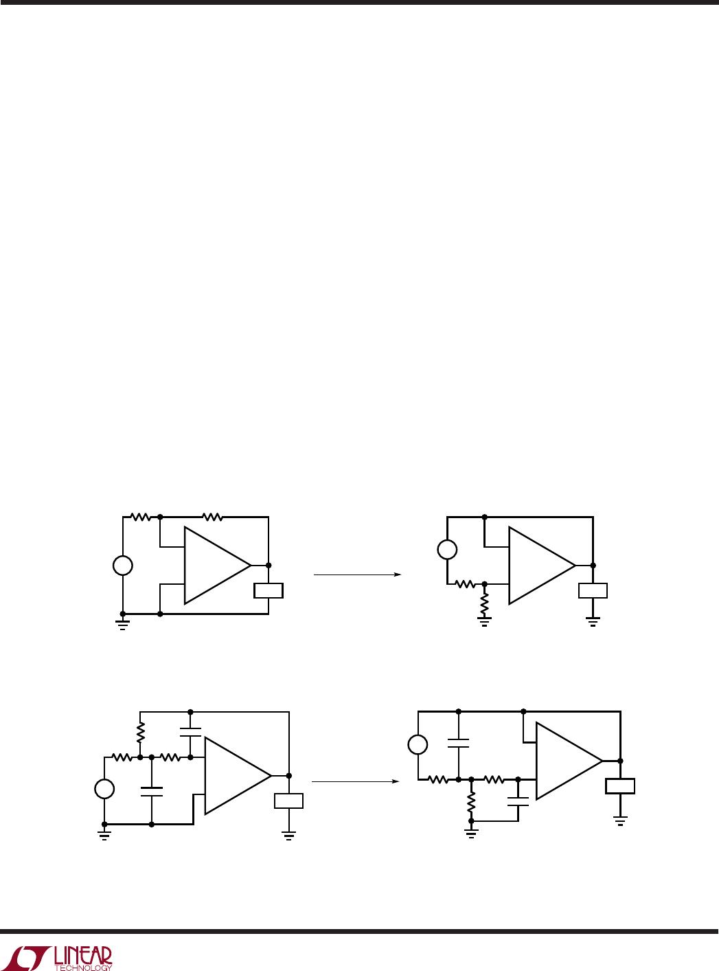
Output Amplifier/Driver
The normalized PWM signal output on the BG
OUT
pin is
converted to the final ring tone signal by an active filter.
This filter consists of an onboard amplifier and a few
external components. Although many different types of
filters can be constructed, a 2-pole Multiple Feedback
(MFB) configuration generally provides adequate perfor-
mance and is desirable due to its simplicity and effective-
ness.
The low frequency component of the ±1.25V PWM signal
contains the desired ring tone frequency and cadence
information. The MFB active filter strips this information
from the PWM signal and amplifies this low frequency
component to generate the final desired output.
Active Tracking Supplies
Implementation of the active tracking supply technique
enables linear generation of the ring tone output, and takes
advantage of the intrinsic supply noise immunity of a
linear amplifier, reducing the need for large high voltage
filtering elements.
Two external power MOSFETs act as voltage level-shifting
devices and generate the power supply voltages for the
LT1684. The LT1684 uses its own output as a voltage
reference for the FET level shifters, “suspending” itself (by
these generated supply voltages) about the signal output.
In this manner, the LT1684 can linearly generate a signal
hundreds of volts in amplitude at its output, while main-
taining ±10V local supply rails across the IC itself.
(Refer to Functional Block Diagram)
* Contact Linear Technology for code.
OPERATIO
U
8
LT1684
Encoded PWM Signal Input Basics
The LT1684 accepts a user-supplied PWM carrier that
represents the desired output ring tone signal. This PWM
input is normalized by the LT1684 such that ring tone
output amplitudes can be accurately encoded into the
PWM input.
The LT1684 accepts a differential input to maximize rejec-
tion of system transients and ground noise. If no differen-
tial signal is readily available from the PWM controller, a
simple inverter/buffer block can be used to create the
differential signal required.
Each differential input is internally connected through a 5k
series resistor to back-to-back isolation-base diodes. These
devices internally clamp the differential input signal to
±100mV greater than the input comparator hysteresis
range. The input comparator toggles with a differential
hysteresis equal to that of a standard diode forward
voltage (0.7V nominal). As such, the differential imped-
ance of the input remains high throughout the input
hysteresis region, then reduces to a nominal value of 10k
(7k minimum) as the input is overdriven beyond the
comparator input threshold. A minimum differential input
of 1.6V is specified to assure valid switching.
The PWM signal can be visualized in terms of instanta-
neous ring tone amplitude, normalized to the LT1684
amplitude reference. For a given desired output voltage
V
OUTN
, the input pulse train required follows the relation:
V
OUTN
= 2 • V
REF
• (DC – 0.5), or
DC = [V
OUTN
/ (2 • V
REF
)] + 0.5, where:
V
REF
= 1.25V normalized peak voltage
DC = PWM input duty cycle
A 10% to 90% duty cycle range is a practical limit for a
10kHz input carrier. This corresponds to normalized sig-
nal amplitude of ±1V. Duty cycles exceeding this range can
cause increased output signal distortion as signal energy
is lost due to finite rise and fall times becoming a signifi-
cant percentage of the signal pulses. The associated
reduction in the pulse energy manifests itself as a “soft
clipping” of the output signal resulting in an increase in
harmonic distortion.
The normalized PWM signal is amplified to the desired
output signal level by the active filter/amplifier stage.
Thus, dividing the desired peak output amplitude by the
peak normalized encoded amplitude (V
OUT
/V
OUTN
) yields
the required DC gain of the active filter.
System Considerations
Assuming use of a 10% to 90% maximum PWM range, the
peak normalized signal will be:
V
PWM
(pk) = ± 0.8 • V
REF
= ±1.0V, and:
V
OUT
(pk) = V
PWM
(pk) • Filter DC Gain
Thus, the DC gain of the output filter equals the desired
peak voltage of the output ring tone signal.
The frequency characteristics of the lowpass output filter
must reflect the allowable carrier ripple on the output
signal. For example, a 10kHz carrier system could use a
2-pole Butterworth lowpass with a cutoff frequency of
100Hz. This filter provides 40dB of input signal rejection
at 10kHz yielding 25mV
P-P
output ripple. If the DC gain of
the output filter/amplifier was 100, the output ripple volt-
age would be riding on a ±100V sine wave, and therefore
be about –78dB relative to the output ring signal.
APPLICATIO S I FOR ATIO
WUUU
9
LT1684
For applications that are extremely output ripple sensitive,
additional carrier rejection can be accomplished by modi-
fying the output filter/amplifier characteristics such as
implementing elliptical filter characteristics with a lower
cutoff frequency or implementation of additional poles.
Filter Design and Component Selection
The ring tone information represented in the low fre-
quency component of the input PWM signal is retrieved
using an active filter. This filter also generates the appro-
priate low frequency gain required to produce the high
voltage output signal and references the output to ground
(or other system reference). The frequency and gain
characteristics of this circuit element are both configurable
by the appropriate choice of external passive filter ele-
ments. Because of the active tracking supply mode of
operation, conventional active filter topologies cannot be
used. Most amplifier/filter topologies can, however, be
“transformed” into active tracking supply topologies.
A conventional amplifier circuit topology can be “trans-
formed” into an active tracking supply amplifier circuit by:
a) Inverting the amplifier signal polarity (swap amplifier +
and – connections) and input source polarity.
b) Referencing all signals to the output except the feed-
back elements, which are referenced to ground (swap
output and ground).
A variety of amplifier/filter configurations can be realized
using the transformation technique. A 2-pole filter is
generally adequate for most ringer applications. Due to the
relative simplicity of infinite-gain Multiple Feedback (MFB)
configurations, these filters are good candidates for ringer
applications. Component selection and active tracking
supply transformation will be described for the following
2-pole MFB infinite-gain lowpass filter.
+
+
V
IN
R1 R2
LOAD
+
+
V
IN
R1
TRANSFORMATION
Conventional Amplifier Configuration Active Tracking Supply Amplifier
Lowpass Mulitple Feedback Active Filter Active Tracking Supply Lowpass
Multiple Feedback Filter
R2
LOAD
TRANSFORMATION
+
+
V
IN
R1 R3
C1
LOAD
C2R2
+
R3R1
1684 F01
LOAD
C2
C1
R2
+
V
IN
APPLICATIO S I FOR ATIO
WUUU

LT1684IS#TRPBF

Mfr. #:
Manufacturer:
Analog Devices / Linear Technology
Description:
Gate Drivers uP Ring Tone Gen
Lifecycle:
New from this manufacturer.
Delivery:
DHL FedEx Ups TNT EMS
Payment:
T/T Paypal Visa MoneyGram Western Union