Technical Note
BU1571KN
3/8
www.rohm.com
2010.06 - Rev.C
© 2010 ROHM Co., Ltd. All rights reserved.
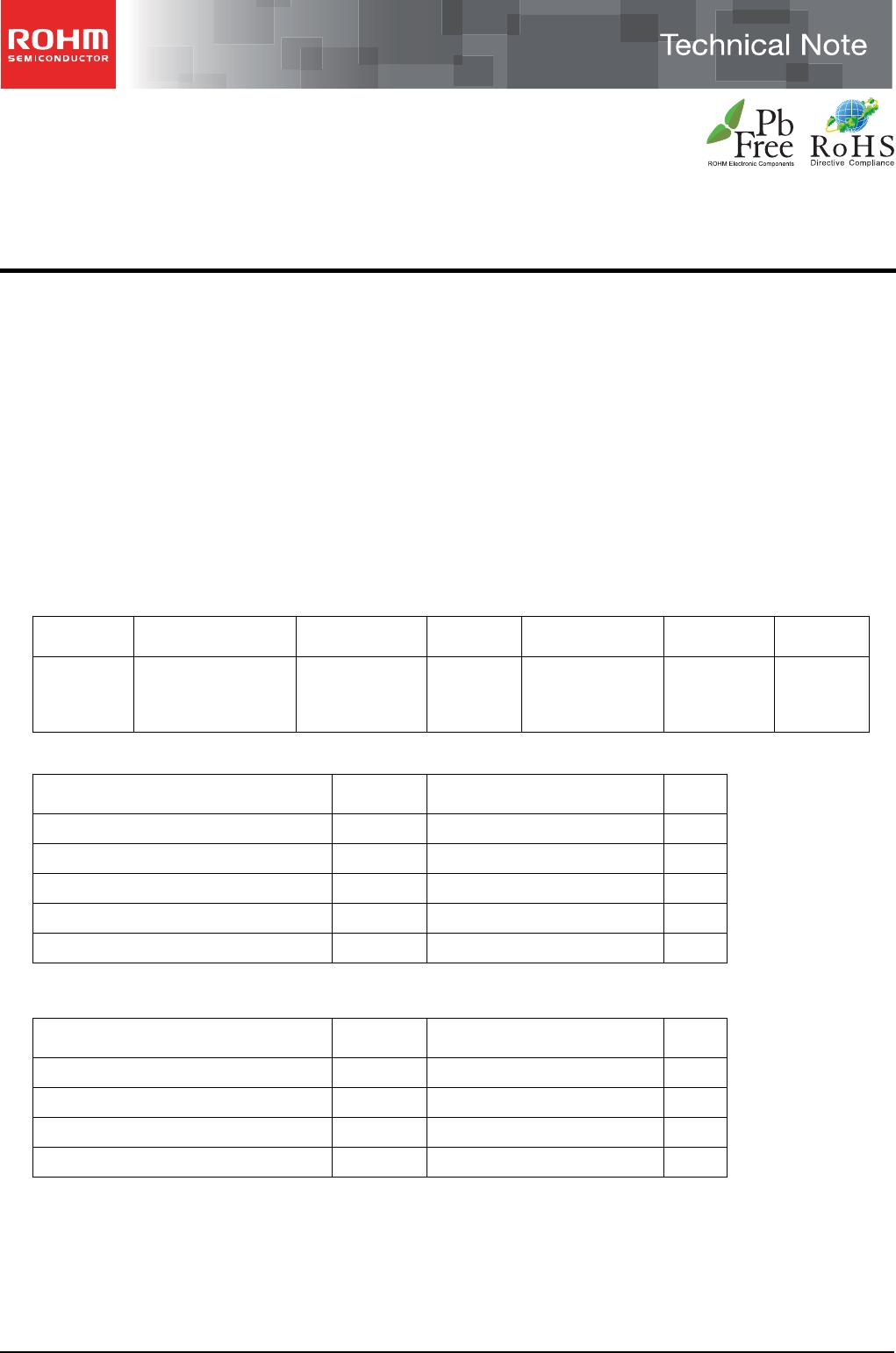
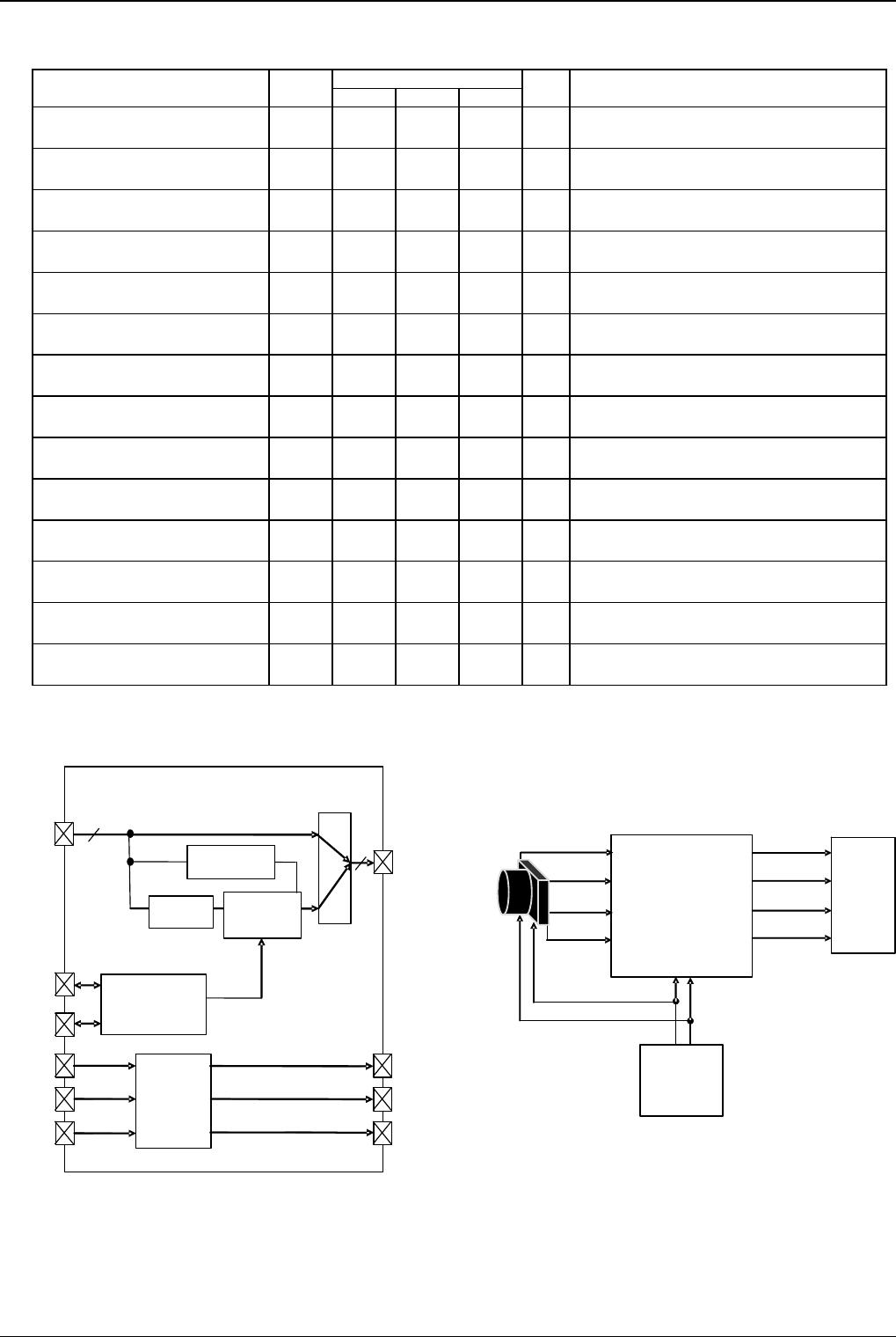
●Terminal functions
PIN No. PIN Name In/Out Active Level Init Function explanation I/O type
1 CAMVSI In * - Vertical Timing Input (pull-down at sleep mode) B*1
2 N.C.
3 CAMHSI In * - Horizontal Timing Input (pull-down at sleep mode) B*1
4 CAMDI0 In DATA - Data Input Bit 0 (pull-down at sleep mode) B*1
5 CAMDI1 In DATA - Data Input Bit 1 (pull-down at sleep mode) B*1
6 CAMDI2 In DATA - Data Input Bit 2 (pull-down at sleep mode) B*1
7 CAMDI3 In DATA - Data Input Bit 3 (pull-down at sleep mode) B*1
8 CAMDI4 In DATA - Data Input Bit 4 (pull-down at sleep mode) B*1
9 CAMDI5 In DATA - Data Input Bit 5 (pull-down at sleep mode) B*1
10 CAMDI6 In DATA - Data Input Bit 6 (pull-down at sleep mode) B*1
11 CAMDI7 In DATA - Data Input Bit 7 (pull-down at sleep mode) B*1
12 VDDIO - PWR - DIGITAL IO Power Source -
13 CAMCKI In CLK - Clock Input (pull-down at sleep mode) D*1
14 GND - GND - Common GROUND -
15 VDD - PWR - CORE Power Source -
16 SDA In/Out DATA In In/Output Serial Data E
17 SDC In/Out CLK In In/Output Serial Clock E
18 TESTOUT Out High - TEST Out Pin ( Keep Open ) -
19 CAMVSO Out - - Vertical Timing Signal Output C
20 N.C.
21 CAMHSO Out - - Horizontal Timing Signal Output C
22 CAMDO0 Out DATA - Data Output: Bit 0 C
23 CAMDO1 Out DATA - Data Output: Bit 1 C
24 CAMDO2 Out DATA - Data Output: Bit 2 C
25 CAMDO3 Out DATA - Data Output: Bit 3 C
26 CAMDO4 Out DATA - Data Output: Bit 4 C
27 CAMDO5 Out DATA - Data Output: Bit 5 C
28 CAMDO6 Out DATA - Data Output: Bit 6 C
29 CAMDO7 Out DATA - Data Output: Bit 7 C
30 TEST1 In Low - Test Mode Terminal 1 (Connect to GND) B
31 TEST2 In Low - Test Mode Terminal 2 (Connect to GND) B
32 RESETB In Low - System Reset Signal A
33 VDDIO - PWR - DIGITAL IO Power Source -
34 CAMCKO Out CLK - Clock Output C
35 GND - GND - Common GROUND -
36 VDD - PWR - CORE Power Source -
*”*” in the Active Level column indicates that it may be changed during set-up of the register. Init indicates pin status when released from reset.
*1: Pull-down is ON during reset (initial status).