PDF: 09005aef80a8e793/Source: 09005aef80a8e767 Micron Technology, Inc., reserves the right to change products or specifications without notice.
dd5c16_32x72h.fm - Rev. F 2/07 EN
13 ©2004 Micron Technology, Inc. All rights reserved.
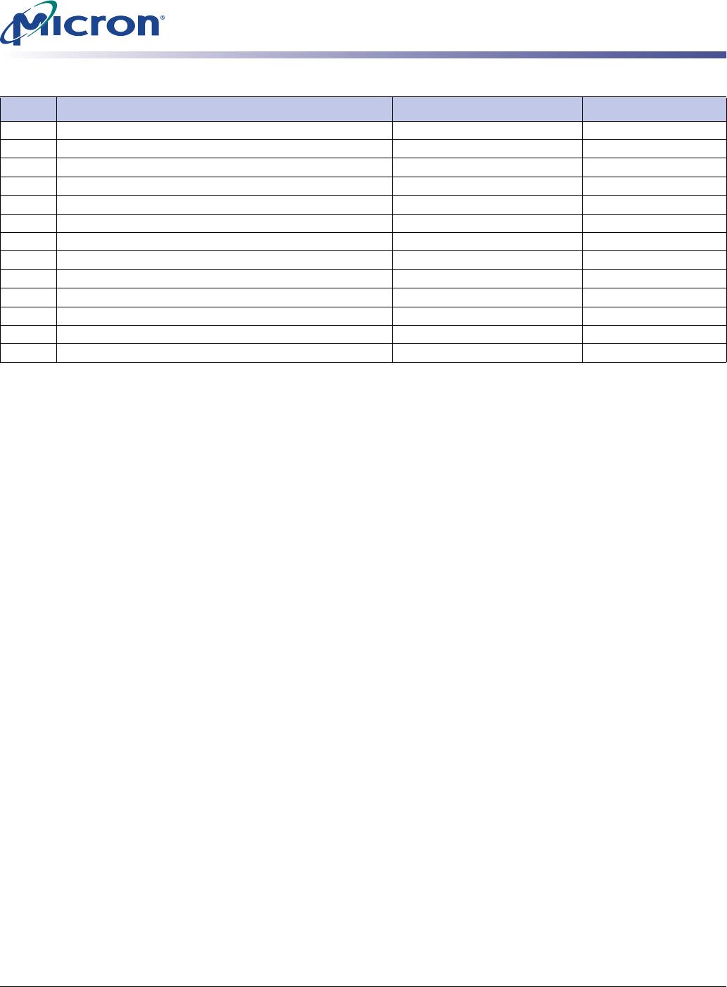
128MB, 256MB: (x72, ECC, SR) 200-Pin DDR SODIMM
Serial Presence-Detect
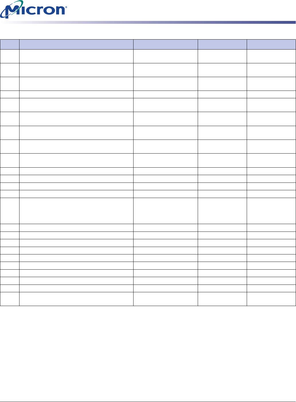
Notes: 1. The value for -26A
t
CK set to 7ns (0 x 70) for optimum BIOS compatibility. Actual device
specification value is 7.5ns.
2. The value of
t
RAS used for -262/-26A/-265 modules is calculated from
t
RC -
t
RP. Actual device
specification value is 40ns.
3. The JEDEC SPD specification allows fast or slow slew rate values for these bytes. The worst-
case (slow slew rate) value is represented here. Systems requiring the fast slew rate setup
and hold values are supported, provided the faster minimum slew rate is met.
4. The value of
t
RP,
t
RCD, and
t
RAP for -335 modules indicated as 18ns to align with industry
specifications; actual DDR SDRAM device specification is 15ns.
33
Address and command hold time,
t
IH
3
0.8ns (-335)
1.0ns (-262/-26A/-265)
80
A0
80
A0
34
Data/data mask input setup time,
t
DS
0.45ns (-335)
0.5ns (-262/-26A/-265)
45
50
45
50
35
Data/data mask input hold time,
t
DH
0.45ns (-335)
0.5ns (-262/-26A/-265)
45
50
45
50
36–40
Reserved
00000
41
MIN active-to-active/refresh time,
t
RC
60ns (-335/-262)
65ns (-26A/-265)
3C
41
3C
41
42
MIN AUTO REFRESH-to-ACTIVE/AUTO
REFRESH command period,
t
RFC
72ns (-335)
75ns (-262/-26A/-265)
48
4B
48
4B
43
SDRAM device MAX cycle time,
t
CK (MAX)
12ns (-335)
13ns (-262/-26A/-265)
30
34
30
34
44
SDRAM device MAX DQS–DQ skew time,
t
DQSQ
0.45ns (-335)
0.5ns (-262/-26A/-265)
2D
32
2D
32
45
SDRAM device MAX read data hold skew
factor,
t
QHS
0.55ns (-335)
0.75ns (-262/-26A/-265)
55
75
55
75
46
Reserved
00000
47
DIMM height
01 01
48–61
Reserved
00000
62
SPD revision
Release 1.0 10 10
63
Checksum for bytes 0–62
-335
-262
-26A
-265
29
BC
E9
19
4A
DD
0A
3A
64
Manufacturer’s JEDEC ID code
MICRON 2C 2C
65–71
Manufacturer’s JEDEC ID code
(continued) 00 00
72
Manufacturing location
1–12 01–0C 01–0C
73–90
Module part number (ASCII)
– Variable data Variable data
91
PCB identification code
1–9 01–09 01–09
92
Identification code (continued)
00000
93
Year of manufacture in BCD
– Variable data Variable data
94
Week of manufacture in BCD
– Variable data Variable data
95–98
Module serial number
– Variable data Variable data
99–
127
Reserved for manufacturer-specific data
00 00
Table 13: Serial Presence-Detect Matrix (-335, -26A, and -265 Speed Grades) (continued)
Byte Description Entry (Version) 128MB 256MB