Data Sheet ADuM6132
0
1
2
3
4
5
6
0
200
400 600
800 1000
07393-030
V
OA
DATA FREQUENCY (kHz)
I
DDA
CURRENT (mA)
V
DDA
= 12.5V
V
DDA
= 15V
V
DDA
= 17V
Figure 10. Typical I
DDA
Supply Current, C
L
= 200 pF
0
1
2
3
4
5
6
0
200 400 600 800
1000
07393-031
V
OB
DATA FREQUENCY (kHz)
I
DDB
CURRENT (mA)
V
DDB
= 12.5V
V
DDB
= 15V
V
DDB
= 17V
Figure 11. Typical I
DDB
Supply Current, C
L
= 200 pF
–5
–4
–3
–2
–1
0
50 100 150 200 250
0
07393-032
I
OH
(mA)
(V
OH
– V
DD
) OUTPUT VOLTAGE DROP (V)
Figure 12. Typical V
OH
Voltage Drop vs. I
OH
(V
DD
= V
DDL
= 5 V,
V
DDA
= V
DDB
= 12 V to 17 V)
0
1
2
3
4
50
100
150
200 250
0
07393-033
I
OL
(mA)
V
OL
OUTPUT VOLTAGE (V)
Figure 13. Typical V
OL
vs. I
OL
(V
DD
= V
DDL
= 5 V, V
DDA
= V
DDB
= 12 V to 17 V)
50
55
60
65
70
–50 –25 0 25 50 75 100
07393-034
TEMPERATURE (°C)
V
OA
PROPAGATION DELAY (ns)
t
PHL
CHA
t
PLH
CHA
Figure 14. Typical Channel A Propagation Delay vs. Temperature
t
PHL
CHB
t
PLH
CHB
50
55
60
65
70
–50 –25 0 25 50 75 100
07393-035
TEMPERATURE (°C)
V
OB
PROPAGATION DELAY (ns)
Figure 15. Typical Channel B Propagation Delay vs. Temperature
Rev. B | Page 9 of 16
ADuM6132 Data Sheet
TERMINOLOGY
Channel-to-Channel Matching
Channel-to-channel matching with rising or falling matching
edge polarity is the magnitude of the propagation delay differ-
ence between two channels of the same part when the inputs
are both rising edges or both falling edges. The loads on each
channel are equal.
Channel-to-channel matching with rising vs. falling opposite
edge polarity is the magnitude of the propagation delay differ-
ence between two channels of the same part when one input is
a rising edge and one input is a falling edge. The loads on each
channel are equal.
Maximum Output Current
The maximum output current is the maximum isolated supply
current that the ADuM6132 can provide. This current supports
external loads as well as the needs of the ADuM6132 Channel A
output circuitry. This is achieved
via external connection of the
V
ISO
pin to the V
DDA
pin and of the GND
ISO
pin to the GND
A
pin
(see Figure 16). The net current available to power external loads
is the A
DuM6132 output current, I
ISO
, minus the Channel A
supply current, I
DDA
.
Maximum Switching Frequency
The maximum switching frequency is the maximum signal
frequency at which the specified timing parameters are guar-
anteed. Operation beyond the maximum switching frequency
is not recommended, because high switching rates can cause
droop in the output supply voltage.
Minimum Pulse Width
The minimum pulse width is the shortest pulse width at which
the specified pulse width distortion is guaranteed. Operation
below the minimum pulse width is not recommended.
Part-to-Part Matching
Part-to-part matching is the magnitude of the propagation
delay difference between the same channels of two different
parts. This includes rising vs. rising edges, falling vs. falling
edges, or rising vs. falling edges. The supply voltages, temp-
eratures, and loads of each part are equal.
Propagation Delay
The propagation delay is the time that it takes a logic signal to
propagate through a component. The propagation delay to a
logic low output may differ from the propagation delay to a
logic high output.
The t
PHL
propagation delay is measured from the 50% level
of the falling edge of the V
IA
or V
IB
signal to the 50% level of
the falling edge of the V
OA
or V
OB
signal. The t
PLH
propagation
delay is measured from the 50% level of the rising edge of the
V
IA
or V
IB
signal to the 50% level of the rising edge of the V
OA
or V
OB
signal.
Capacitive Load (C
L
)
The output capacitive load simulates a typical FET, IGBT, or
buffer for timing or current measurements. This load includes
all discrete and parasitic capacitive loads on the output.
Rev. B | Page 10 of 16
Data Sheet ADuM6132
APPLICATIONS INFORMATION
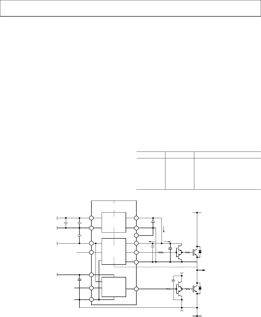
TYPICAL APPLICATION USAGE
The architecture of the ADuM6132 is ideal for motor drive and
inverter applications where the low-side channels are common
to the controller. This arrangement requires only two isolation
regions in a package. All the isolated signals and the isolated
power are grouped on one side of the package to maintain full
package creepage and clearance. The low-side driver, as well as the
control signals, share a common reference and are also grouped.
To maximize the effectiveness of external bypass capacitors, the
isoPower dc-to-dc converter is not internally tied to the data
channels, and should be treated as a completely independent
subsystem, except for a UVLO function (see the Undervoltage
Lockout section). This means that power must be applied to V
DD
to operate the dc-to-dc converter. Power must also be applied to
V
DDL
and V
DDB
to operate the data input and the Channel B
driver output. On the secondary side, the power generated at
the V
ISO
pin must be applied as an input power supply to the
V
DDA
pin. GND
ISO
and GND
A
must also be connected.
The ADuM6132 is intended for use in driving low gate
capacitance transistors (200 pF typically). Most high voltage
applications involve larger transistors than this. To accom-
modate these applications, users can implement a buffer
configuration with the ADuM6132, as shown in Figure 16. In
many cases, this buffer configuration is the least expensive
option to drive high capacitance devices and provides the
greatest amount of design flexibility. The precise buffer/high
voltage transistor combination can be selected to suit the
requirements of the application.
PCB LAYOUT
The ADuM6132 digital isolator with integrated 275 mW
isoPower dc-to-dc converter requires no external interface
circuitry for the logic interfaces. Power supply bypassing is
required at the input and output supply pins (see Figure 17).
The power supply section of the ADuM6132 uses a very high
oscillator frequency to efficiently pass power through its chip
scale transformers. In addition, the normal operation of the
data section of the iCoupler introduces switching transients
on the power supply pins. Bypass capacitors are required for
several operating frequencies. Noise suppression requires a low
ESR, high frequency capacitor; ripple suppression and proper
regulation require a large value capacitor in parallel (see Table 10).
The total lead length between both ends of the capacitor and
the input power supply pin should not exceed 20 mm.
Table 10. Recommended Bypass Capacitors
Supply Pins Bypass Capacitors
V
DD
1, 2 0.1 μF, 10 μF
V
DDB
7, 8 0.1 μF
V
DDL
2, 3 0.1 μF
V
DDA
13, 14 0.1 μF
V
ISO
15, 16 0.1 μF, 10 μF
+5V
+15V
V
DD
GND
V
ISO
GND
ISO
1
2
V
DDL
3
V
IA
4
V
DDB
7
GND
8
16
15
GND
ISO
9
GND
A
14
V
DDA
13
V
OA
12
ISOLATED
DC-TO-DC
CONVERTER
ISOLATED
GATE
DRIVE
NONISOLATED
GATE
DRIVE
ADuM6132
0.1µF
0.1µF
0.1µF
10µF
+5V
GND
V
IB
5
R
G
I
DDA
I
AVAIL
I
ISO
R
BUF
C
BUF
0.1µF
BUFFER
BUFFER
V
DC+
V
DC–
R
G
R
BUF
C
BUF
+15V
GND
V
OB
6
07393-016
0.1µF
Figure 16. Typical Application Circuit
Rev. B | Page 11 of 16

ADUM6132ARWZ

Mfr. #:
Manufacturer:
Analog Devices Inc.
Description:
Digital Isolators Half-Bridge Dvr w/ Intg Hi-Side Supply
Lifecycle:
New from this manufacturer.
Delivery:
DHL FedEx Ups TNT EMS
Payment:
T/T Paypal Visa MoneyGram Western Union

Products related to this Datasheet