ADuM6132 Data Sheet
In applications involving high common-mode transients, care
should be taken to ensure that board capacitive coupling across
the isolation barrier is minimized. Furthermore, the board
layout should be designed so that any coupling that does occur
affects all pins on a given component side equally. Failure to
ensure this may cause voltage differentials between pins that
exceed the absolute maximum ratings of the device (see Table 7),
leading to latch-up or permanent damage.
V
DD
GND
V
DDL
V
IA
V
ISO
GND
ISO
GND
A
V
DDA
V
IB
V
OA
V
OB
NC
V
DDB
NC
GND GND
ISO
07393-017
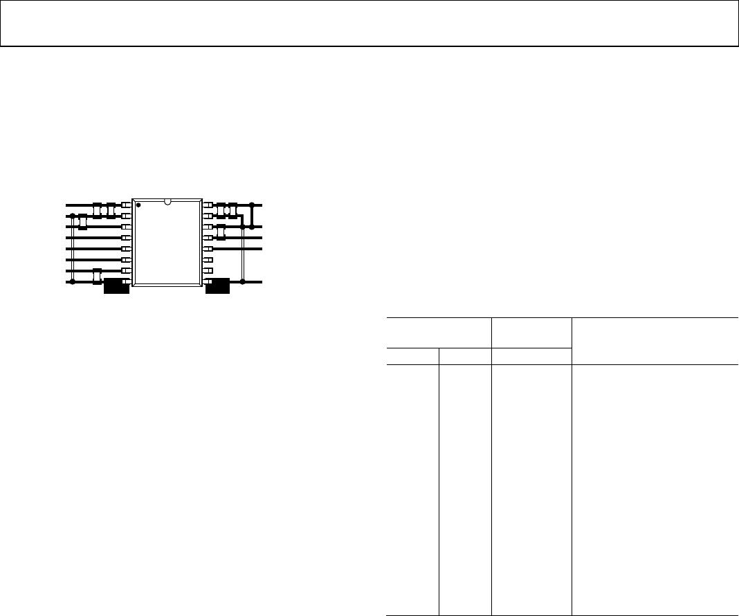
Figure 17. Recommended PCB Layout
The ADuM6132 is a power device that dissipates approximately
1 W of power when fully loaded and running at maximum speed.
Because it is not possible to apply a heat sink to an isolation
device, the device depends primarily on heat dissipation into
the PCB through the GND pins. If the device will be used at
high ambient temperatures, provide a thermal path from the
GND pins to the PCB ground plane.
The board layout in Figure 17 shows enlarged pads for Pin 8
(GND) and Pin 9 (GND
ISO
). Multiple vias should be implemented
from the pad to the ground plane. This layout significantly reduces
the temperatures inside the chip. The dimensions of the expanded
pads are left to the discretion of the designer and the available
board space. See the AN-0971 Application Note for board
layout recommendations.
THERMAL ANALYSIS
The ADuM6132 consists of several internal die attached to
two lead frame paddles. For the purposes of thermal analysis,
the part is treated as a thermal unit with the highest junction
temperature determining θ
JA
, as shown in Ta ble 2 . The value of
θ
JA
is based on measurements taken with the part mounted on
a JEDEC standard 4-layer board with fine width traces and still
air. Under normal operating conditions, the ADuM6132 oper-
ates at full load across the full temperature range without derating
the output current. However, following the recommendations in
the PCB Layout section decreases the thermal resistance to the
PCB, allowing increased thermal margin at high ambient
temperatures.
Under V
ISO
output short-circuit conditions, as shown in
Figure 9, the package power dissipation quickly exceeds the safe
operating limit of 1.44 W for ambient temperatures up to 85°C.
At low input voltage, the power dissipation can approach 2 W.
Because internal compensation of the PWM makes low V
DD
a
worst-case condition, input voltage limiting is not an effective
strategy for protecting the ADuM6132 from output load fault
conditions. Therefore, the preferred protection methods, where
required, are either limiting ambient temperature to 60°C or the
use of a fuse.
UNDERVOLTAGE LOCKOUT
The ADuM6132 has undervoltage lockout (UVLO) circuits on
the V
DDL
, V
DDA
, and V
DDB
supplies. For each supply, the respective
UVLO circuit monitors the supply voltage and takes a predeter-
mined action based on whether the supply voltage is above or
below a given threshold. These thresholds are specified in Table 1.
In the recommended configuration shown in Figure 16, only
two independent supplies are controlled by the user: V
DDB
and
V
DDL
/V
DD
(V
DDL
= V
DD
in Figure 16). V
DDA
is supplied by the
internal dc-to-dc converter via the V
ISO
= V
DDA
external connec-
tion. Nevertheless, the V
DDA
UVLO functionality is included in
Table 11 to show how the V
OA
output behaves when the internal
dc-to-dc converter powers on and off.
Table 11. Undervoltage Lockout Functionality
1
User-Provided
Supplies
V
ISO
Powered
Supply
V
DDL
V
DDB
V
DDA
Effect
H H H Normal operation.
Internal dc-to-dc converter is
active.
V
OA
/V
OB
output logic states
match V
IA
/V
IB
input logic states.
H H L Internal dc-to-dc converter is
active but V
ISO
is below UVLO
threshold.
V
OA
output is driven low.
V
OB
output operates normally.
X L X Internal dc-to-dc converter is
turned off (V
ISO
= 0 V).
V
OA
output is driven low.
V
OB
output is driven low.
L X X Internal dc-to-dc converter is
turned off (V
ISO
= 0 V).
V
OA
output is driven low.
V
OB
output is driven low.
1
H: supply voltage > UVLO threshold; L: supply voltage < UVLO threshold;
X: supply voltage level is irrelevant.
When all three supplies are above their respective UVLO
thresholds, the ADuM6132 operates normally. The internal
dc-to-dc converter is active, and both outputs operate as
determined by their respective input logic signals. If either of
the user-provided supplies is below its UVLO threshold, the
ADuM6132 is put into a disabled mode. In this mode, the
internal dc-to-dc converter is turned off and both outputs are
driven low.
The V
OB
output is driven low by either the V
DDL
or V
DDB
UVLO circuit (whichever is below its threshold). The V
OA
output is driven low when the internal dc-to-dc converter is
turned off. The V
ISO
supply voltage drops to 0 V, causing V
DDA
to drop also because V
ISO
and V
DDA
are externally connected.
When V
DDA
is below its UVLO threshold, the V
DDA
UVLO
circuit drives V
OA
low.
Rev. B | Page 12 of 16
Data Sheet ADuM6132
PROPAGATION DELAY-RELATED PARAMETERS
Propagation delay is a parameter that describes the time it takes
a logic signal to propagate through a component. The propaga-
tion delay to a logic low output may differ from the propagation
delay to a logic high output.
INPUT (V
Ix
)
OUTPUT (V
Ox
)
t
PLH
t
PHL
50%
50%
07393-018
Figure 18. Propagation Delay Parameters
Pulse width distortion is the maximum difference between
these two propagation delay values and is an indication of how
accurately the timing of the input signal is preserved.
Channel-to-channel matching refers to the maximum amount
that the propagation delay differs between channels within a
single ADuM6132 component.
MAGNETIC FIELD IMMUNITY
The ADuM6132 is extremely immune to external magnetic
fields. The limitation on the ADuM6132 magnetic field immunity
is set by the condition in which induced voltage in the receiving
coil of the transformer is sufficiently large to falsely set or reset
the decoder. The following analysis defines the conditions
under which this may occur.
The pulses at the transformer output have an amplitude greater
than 1.0 V. The decoder has a sensing threshold at approximately
0.5 V, thus establishing a 0.5 V margin in which induced voltages
can be tolerated. The voltage induced across the receiving coil is
given by
V = (−/dt) Σπr
n
2
; n = 1, 2, … N
where:
β is the magnetic flux density (gauss).
r
n
is the radius of the nth turn in the receiving coil (cm).
N is the number of turns in the receiving coil.
Given the geometry of the receiving coil in the ADuM6132 and
an imposed requirement that the induced voltage be at most
50% of the 0.5 V margin at the decoder, a maximum allowable
magnetic flux density is calculated, as shown in Figure 19.
MAGNETIC FIELD FREQUENCY (Hz)
100
MAXIMUM ALLOWABLE MAGNETIC FLUX
DENSITY (kgauss)
0.001
1M
10
0.01
1k
10k 10M
0.1
1
100M100k
07393-019
Figure 19. Maximum Allowable External Magnetic Flux Density
For example, at a magnetic field frequency of 1 MHz, the
maximum allowable magnetic flux density of 0.2 kgauss
induces a voltage of 0.25 V at the receiving coil. This voltage
is approximately 50% of the sensing threshold and does not
cause a faulty output transition. Similarly, if such an event
occurs during a transmitted pulse (with the worst-case polarity),
the received pulse is reduced from >1.0 V to 0.75 Vstill well
above the 0.5 V sensing threshold of the decoder.
The preceding magnetic flux density values correspond to
specific current magnitudes at given distances from the
ADuM6132 transformers. Figure 20 expresses these allowable
current magnitudes as a function of frequency for selected
distances. As shown in Figure 20, the ADuM6132 is extremely
immune and can be affected only by extremely large currents
operated at high frequency and very close to the component.
For example, at a magnetic field frequency of 1 MHz, a 0.5 kA
current would need to be placed 5 mm away from the ADuM6132
to affect the operation of the component.
MAGNETIC FIELD FREQUENCY (Hz)
MAXIMUM ALLOWABLE CURRENT (kA)
1000
100
10
1
0.1
0.01
1k 10k 100M
100k 1M 10M
DISTANCE = 5mm
DISTANCE = 1m
DISTANCE = 100mm
07393-020
Figure 20. Maximum Allowable Current for Various
Current-to-ADuM6132 Spacings
Rev. B | Page 13 of 16
ADuM6132 Data Sheet
Note that in the presence of strong magnetic fields and high
frequencies, any loops formed by PCB traces may induce
sufficiently large error voltages to trigger the threshold of
succeeding circuitry. Care should be taken in the layout of such
traces to avoid this possibility.
INSULATION LIFETIME
All insulation structures eventually break down when subjected
to voltage stress over a sufficiently long period. The rate of insu-
lation degradation depends on the characteristics of the voltage
waveform applied across the insulation. In addition to the testing
performed by the regulatory agencies, Analog Devices conducts
an extensive set of evaluations to determine the lifetime of the
insulation structure within the ADuM6132.
Analog Devices performs accelerated life testing using voltage
levels higher than the rated continuous working voltage. Accel-
eration factors for several operating conditions are determined.
These factors allow calculation of the time to failure at the actual
working voltage. Table 12 summarizes the recommended peak
working voltages for 50 years and 15 years of service life for
various operating conditions evaluated by Analog Devices. In
many cases, the approved working voltage is higher than the
50-year service life voltage. Operation at these high working
voltages can lead to shortened insulation life in some cases.
The insulation lifetime of the ADuM6132 depends on the
voltage waveform type imposed across the isolation barrier.
The iCoupler insulation structure degrades at different rates
depending on whether the waveform is bipolar ac, unipolar ac,
or dc. Figure 21, Figure 22, and Figure 23 illustrate these
different isolation voltage waveforms.
Bipolar ac voltage is the most stringent environment. The goal
of a 50-year operating lifetime under the bipolar ac condition
determines the maximum working voltage recommended by
Analog Devices.
In the case of unipolar ac or dc voltage, the stress on the
insulation is significantly lower, which allows operation at
higher working voltages while still achieving a 50-year service
life. The working voltages listed in Table 12 can be applied while
maintaining the 50-year minimum lifetime, provided that the
voltage conforms to either the unipolar ac or dc voltage cases.
Any cross-insulation voltage waveform that does not conform to
Figure 22 or Figure 23 should be treated as a bipolar ac waveform,
and its peak voltage should be limited to the 50-year lifetime
voltage value listed in Table 12. Note that the voltage shown in
Figure 22 is sinusoidal for illustration purposes only. It is meant
to represent any voltage waveform varying between 0 V and
some limiting value. The limiting value can be positive or
negative, but the voltage cannot cross 0 V.
0V
RATED PEAK VOLTAGE
07393-021
Figure 21. Bipolar AC Waveform
0V
RATED PEAK VOLTAGE
07393-022
Figure 22. Unipolar AC Waveform
0V
RATED PEAK VOLTAGE
07393-023
Figure 23. DC Waveform
Table 12. Maximum Continuous Working Voltage
1
Parameter Peak Voltage Lifetime
AC Voltage, Bipolar Waveform 424 V peak 50-year minimum lifetime
AC Voltage, Unipolar Waveform
Basic Insulation 800 V peak 15-year minimum lifetime
Basic Insulation
660 V peak
50-year minimum lifetime
DC Voltage Waveform
Basic Insulation 800 V peak 15-year minimum lifetime
Basic Insulation 660 V peak 50-year minimum lifetime
1
Refers to continuous voltage magnitude imposed across the isolation barrier. See the Insulation Lifetime section for more information.
Rev. B | Page 14 of 16

ADUM6132ARWZ

Mfr. #:
Manufacturer:
Analog Devices Inc.
Description:
Digital Isolators Half-Bridge Dvr w/ Intg Hi-Side Supply
Lifecycle:
New from this manufacturer.
Delivery:
DHL FedEx Ups TNT EMS
Payment:
T/T Paypal Visa MoneyGram Western Union

Products related to this Datasheet