Data Sheet ADuM6132
Rev. B | Page 7 of 16
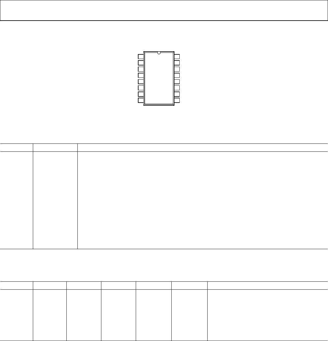
PIN CONFIGURATION AND FUNCTION DESCRIPTIONS
V
DD
1
GND
2
V
DDL
3
V
IA
4
V
ISO
16
GND
ISO
15
GND
A
14
V
DDA
13
V
IB
5
V
OA
12
V
OB
6
NC
11
V
DDB
7
NC
10
GND
8
GND
ISO
9
NC = NO CONNECT
ADuM6132
TOP VIEW
(Not to Scale)
07393-003
Figure 3. Pin Configuration
Table 8. Pin Function Descriptions
Pin No. Mnemonic Description
1 V
DD
Input Supply Voltage for Isolated Power Supply, 4.5 V to 5.5 V.
2, 8 GND
Ground Reference for Isolated Power Supply Input and Logic Inputs.
3 V
DDL
Input Supply Voltage for Logic, 4.5 V to 5.5 V.
4 V
IA
Logic Input A.
5 V
IB
Logic Input B.
6 V
OB
Output B (Nonisolated).
7 V
DDB
Output B Supply Voltage Input (Nonisolated), 12.5 V to 17 V.
9, 15 GND
ISO
Ground Reference for Isolated Power Supply Output.
10, 11 NC No Connect.
12 V
OA
Output A (Isolated).
13 V
DDA
Output A Supply Voltage Input. Must be connected externally to V
ISO
(Pin 16).
14 GND
A
Output A Ground Reference. Must be connected externally to GND
ISO
(Pin 15).
16 V
ISO
Isolated Power Supply Voltage Output.
Table 9. Truth Table (Positive Logic)
1
V
IA
Input V
IB
Input V
DDL
State V
DDB
State V
OA
Output V
OB
Output Notes
L L Powered Powered L L
L H Powered Powered L H
H L Powered Powered H L
H H Powered Powered H H
X X Unpowered Powered L L
V
OA
returns to input state within 1 μs of V
DDL
power restoration
X X Powered Unpowered L L
1
L = low; H = high; X = high or low.