VS-ST780C06L1

VS-ST780CL Series
www.vishay.com
Vishay Semiconductors
Revision: 15-Apr-14
1
Document Number: 94415
For technical questions within your region: DiodesAmericas@vishay.com
, DiodesAsia@vishay.com, DiodesEurope@vishay.com
THIS DOCUMENT IS SUBJECT TO CHANGE WITHOUT NOTICE. THE PRODUCTS DESCRIBED HEREIN AND THIS DOCUMENT
ARE SUBJECT TO SPECIFIC DISCLAIMERS, SET FORTH AT www.vishay.com/doc?91000
Phase Control Thyristors
(Hockey PUK Version), 1350 A
FEATURES
Center amplifying gate
Metal case with ceramic insulator
International standard case TO-200AC (B-PUK)
Designed and qualified for industrial level
Material categorization: For definitions of compliance
please see www.vishay.com/doc?99912
TYPICAL APPLICATIONS
DC motor controls
Controlled DC power supplies
AC controllers
ELECTRICAL SPECIFICATIONS
PRODUCT SUMMARY
Package TO-200AC (B-PUK)
Diode variation Single SCR
I
T(AV)
1350 A
V
DRM
/V
RRM
400 V, 600 V
V
TM
1.31 V
I
GT
100 mA
T
J
-40 °C to 125 °C
TO-200AC (B-PUK)
MAJOR RATINGS AND CHARACTERISTICS
PARAMETER TEST CONDITIONS VALUES UNITS
I
T(AV)
1350 A
T
hs
55 °C
I
T(RMS)
2700 A
T
hs
25 °C
I
TSM
50 Hz 24 400
A
60 Hz 25 600
I
2
t
50 Hz 2986
kA
2
s
60 Hz 2726
V
DRM
/V
RRM
400 to 600 V
t
q
Typical 150 µs
T
J
v -40 to 125 °C
VOLTAGE RATINGS
TYPE NUMBER
VOLTAGE
CODE
V
DRM
/V
RRM
, MAXIMUM REPETITIVE
PEAK AND OFF-STATE VOLTAGE
V
V
RSM
, MAXIMUM
NON-REPETITIVE PEAK VOLTAGE
V
I
DRM
/I
RRM
MAXIMUM
AT T
J
= T
J
MAXIMUM
mA
VS-ST780C..L
04 400 500
80
06 600 700
VS-ST780CL Series
www.vishay.com
Vishay Semiconductors
Revision: 15-Apr-14
2
Document Number: 94415
For technical questions within your region: DiodesAmericas@vishay.com
, DiodesAsia@vishay.com, DiodesEurope@vishay.com
THIS DOCUMENT IS SUBJECT TO CHANGE WITHOUT NOTICE. THE PRODUCTS DESCRIBED HEREIN AND THIS DOCUMENT
ARE SUBJECT TO SPECIFIC DISCLAIMERS, SET FORTH AT www.vishay.com/doc?91000
ABSOLUTE MAXIMUM RATINGS
PARAMETER SYMBOL TEST CONDITIONS VALUES UNITS
Maximum average on-state current
at heatsink temperature
I
T(AV)
180° conduction, half sine wave
double side (single side) cooled
1350 (500) A
55 (85) °C
Maximum RMS on-state current I
T(RMS)
DC at 25 °C heatsink temperature double side cooled 2700
A
Maximum peak, one-cycle
non-repetitive surge current
I
TSM
t = 10 ms
No voltage
reapplied
Sinusoidal half wave,
initial T
J
= T
J
maximum
24 400
t = 8.3 ms 25 600
t = 10 ms
100 % V
RRM
reapplied
20 550
t = 8.3 ms 21 500
Maximum I
2
t for fusing I
2
t
t = 10 ms
No voltage
reapplied
2986
kA
2
s
t = 8.3 ms 2726
t = 10 ms
100 % V
RRM
reapplied
2112
t = 8.3 ms 1928
Maximum I
2
t for fusing I
2
t t = 0.1 to 10 ms, no voltage reapplied 29 860 kA
2
s
Low level value of threshold voltage V
T(TO)1
(16.7 % x π x I
T(AV)
< I < π x I
T(AV)
), T
J
= T
J
maximum 0.80
V
High level value of threshold voltage V
T(TO)2
(I > π x I
T(AV)
), T
J
= T
J
maximum 0.90
Low level value of on-state slope resistance r
t1
(16.7 % x π x I
T(AV)
< I < π x I
T(AV)
), T
J
= T
J
maximum 0.14
mΩ
High level value of on-state slope resistance r
t2
(I > π x I
T(AV)
), T
J
= T
J
maximum 0.13
Maximum on-state voltage V
TM
I
pk
= 3600 A, T
J
= T
J
maximum, t
p
= 10 ms sine pulse 1.31 V
Maximum holding current I
H
T
J
= 25 °C, anode supply 12 V resistive load
600
mA
Typical latching current I
L
1000
SWITCHING
PARAMETER SYMBOL TEST CONDITIONS VALUES UNITS
Maximum non-repetitive rate of rise
of turned-on current
dI/dt
Gate drive 20 V, 20 Ω, t
r
1 μs
T
J
= T
J
maximum, anode voltage 80 % V
DRM
1000 A/µs
Typical delay time t
d
Gate current 1 A, dI
g
/dt = 1 A/μs
V
d
= 0.67 % V
DRM
, T
J
= 25 °C
1.0
µs
Typical turn-off time t
q
I
TM
= 750 A, T
J
= T
J
maximum, dI/dt = 60 A/μs,
V
R
= 50 V, dV/dt = 20 V/μs, gate 0 V 100 Ω, t
p
= 500 μs
150
BLOCKING
PARAMETER SYMBOL TEST CONDITIONS VALUES UNITS
Maximum critical rate of rise of
off-state voltage
dV/dt T
J
= T
J
maximum linear to 80 % rated V
DRM
500 V/µs
Maximum peak reverse and
off-state leakage current
I
RRM
,
I
DRM
T
J
= T
J
maximum, rated V
DRM
/V
RRM
applied 80 mA
VS-ST780CL Series
www.vishay.com
Vishay Semiconductors
Revision: 15-Apr-14
3
Document Number: 94415
For technical questions within your region: DiodesAmericas@vishay.com
, DiodesAsia@vishay.com, DiodesEurope@vishay.com
THIS DOCUMENT IS SUBJECT TO CHANGE WITHOUT NOTICE. THE PRODUCTS DESCRIBED HEREIN AND THIS DOCUMENT
ARE SUBJECT TO SPECIFIC DISCLAIMERS, SET FORTH AT www.vishay.com/doc?91000
Note
The table above shows the increment of thermal resistance R
thJ-hs
when devices operate at different conduction angles than DC
TRIGGERING
PARAMETER SYMBOL TEST CONDITIONS
VALUES
UNITS
TYP. MAX.
Maximum peak gate power
P
GM
T
J
= T
J
maximum, t
p
5 ms
10.0
W
Maximum average gate power
P
G(AV)
T
J
= T
J
maximum, f = 50 Hz, d% = 50
2.0
Maximum peak positive gate current
I
GM
T
J
= T
J
maximum, t
p
5 ms
3.0 A
Maximum peak positive gate voltage
+ V
GM
T
J
= T
J
maximum, t
p
5 ms
20
V
Maximum peak negative gate voltage
- V
GM
5.0
DC gate current required to trigger I
GT
T
J
= -40 °C
Maximum required gate
trigger/current/voltage are the
lowest value which will trigger
all units 12 V anode to cathode
applied
200 -
mAT
J
= 25 °C 100 200
T
J
= 125 °C 50 -
DC gate voltage required to trigger V
GT
T
J
= -40 °C
2.5
-
VT
J
= 25 °C 1.8 3.0
T
J
= 125 °C 1.1 -
DC gate current not to trigger I
GD
T
J
= T
J
maximum
Maximum gate
current/voltage not to trigger
is the maximum value which
will not trigger any unit with
rated V
DRM
anode to cathode
applied
10 mA
DC gate voltage not to trigger V
GD
0.25 V
THERMAL AND MECHANICAL SPECIFICATIONS
PARAMETER SYMBOL TEST CONDITIONS VALUES UNITS
Maximum operating junction temperature range T
J
-40 to 125
°C
Maximum storage temperature range T
Stg
-40 to 150
Maximum thermal resistance, junction to heatsink R
thJ-hs
DC operation single side cooled 0.073
K/W
DC operation double side cooled 0.031
Maximum thermal resistance, case to heatsink R
thC-hs
DC operation single side cooled 0.011
DC operation double side cooled 0.006
Mounting force, ± 10 %
14 700
(1500)
N
(kg)
Approximate weight 255 g
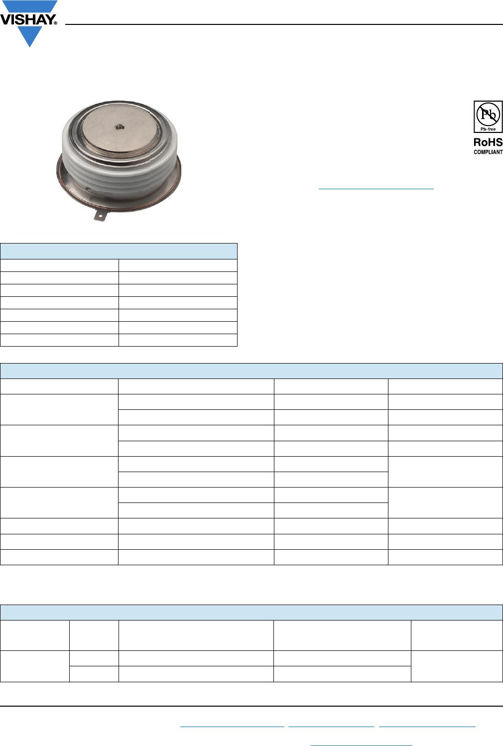
Case style See dimensions - link at the end of datasheet TO-200AC (B-PUK)
ΔR
thJ-hs
CONDUCTION
CONDUCTION ANGLE
SINUSOIDAL CONDUCTION RECTANGULAR CONDUCTION
TEST CONDITIONS UNITS
SINGLE SIDE DOUBLE SIDE SINGLE SIDE DOUBLE SIDE
180° 0.009 0.009 0.006 0.006
T
J
= T
J
maximum K/W
120° 0.011 0.011 0.011 0.011
90° 0.014 0.014 0.015 0.015
60° 0.020 0.020 0.021 0.021
30° 0.036 0.036 0.036 0.036

VS-ST780C06L1

Mfr. #:
Manufacturer:
Vishay Semiconductors
Description:
SCR Modules 1350 Amp 600 Volt 2700 Amp IT(RMS)
Lifecycle:
New from this manufacturer.
Delivery:
DHL FedEx Ups TNT EMS
Payment:
T/T Paypal Visa MoneyGram Western Union