©2011 Silicon Storage Technology, Inc. S725081A 10/11
10
1 Mbit SPI Serial Flash
SST25VF010A
Data Sheet
Microchip Technology Company
Read (20 MHz)
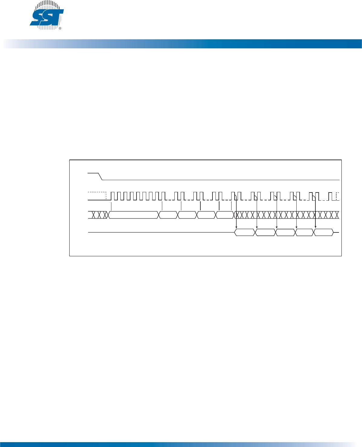
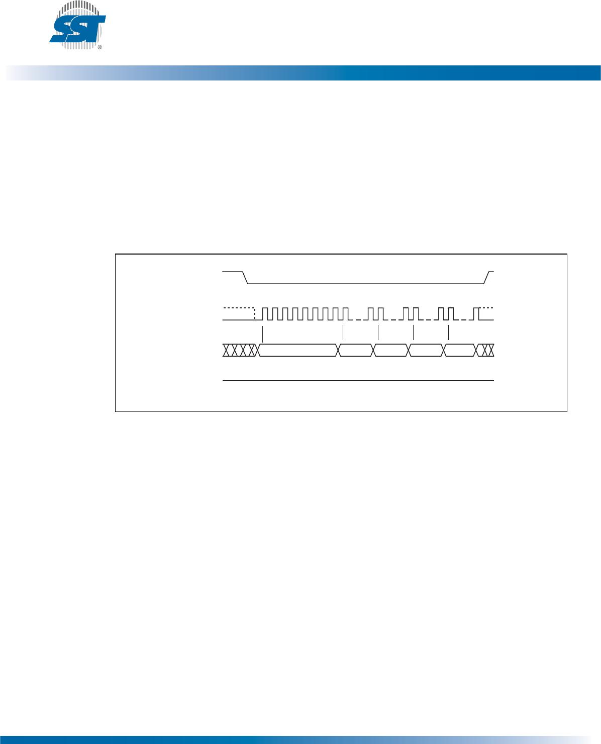
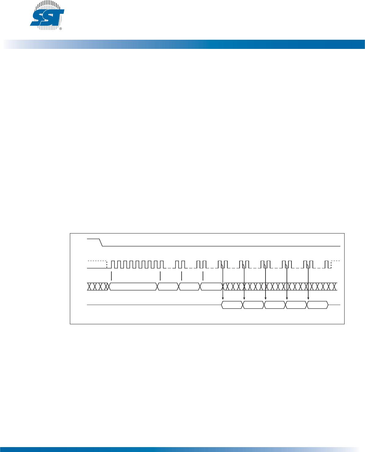
The Read instruction outputs the data starting from the specified address location. The data output
stream is continuous through all addresses until terminated by a low to high transition on CE#. The
internal address pointer will automatically increment until the highest memory address is reached.
Once the highest memory address is reached, the address pointer will automatically increment to the
beginning (wrap-around) of the address space, i.e. for 4 Mbit density, once the data from address loca-
tion 7FFFFH had been read, the next output will be from address location 00000H.
The Read instruction is initiated by executing an 8-bit command, 03H, followed by address bits [A
23
-
A
0
]. CE# must remain active low for the duration of the Read cycle. See Figure 4 for the Read
sequence.
Figure 4: Read Sequence
6. Prior to any Byte-Program, AAI-Program, Sector-Erase, Block-Erase, or Chip-Erase operation, the Write-Enable
(WREN) instruction must be executed.
7. Block addresses for: use A
MS
-A
15
, remaining addresses can be V
IL
or V
IH
8. To continue programming to the next sequential address location, enter the 8-bit command, AFH,
followed by the data to be programmed.
9. The Read-Status-Register is continuous with ongoing clock cycles until terminated by a low to high transition on CE#.
10. The Enable-Write-Status-Register (EWSR) instruction and the Write-Status-Register (WRSR) instruction must work in
conjunction of each other. The WRSR instruction must be executed immediately (very next bus cycle) after the EWSR
instruction to make both instructions effective.
11. Manufacturer’s ID is read with A
0
=0, and Device ID is read with A
0
=1. All other address bits are 00H. The Manufac-
turer’s and Device ID output stream is continuous until terminated by a low to high transition on CE#
12. Device ID = 49H for SST25VF010A
1265 F04.0
CE#
SO
SI
SCK
ADD.
012345678
ADD. ADD.
03
HIGH IMPEDANCE
15 16
23
24
31
32
39
40
7047 48 55 56 63 64
N+2 N+3 N+4N N+1
D
OUT
MSB
MSB
MSB
MODE 0
MODE 3
D
OUT
D
OUT
D
OUT
D
OUT