©2011 Silicon Storage Technology, Inc. S725081A 10/11
13
1 Mbit SPI Serial Flash
SST25VF010A
Data Sheet
Microchip Technology Company
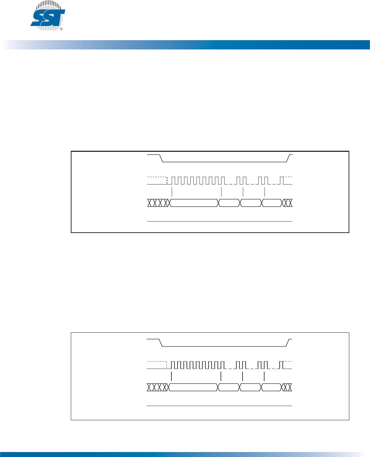
Auto Address Increment (AAI) Program
The AAI program instruction allows multiple bytes of data to be programmed without re-issuing the
next sequential address location. This feature decreases total programming time when the entire mem-
ory array is to be programmed. An AAI program instruction pointing to a protected memory area will be
ignored. The selected address range must be in the erased state (FFH) when initiating an AAI program
instruction.
Prior to any write operation, the Write-Enable (WREN) instruction must be executed. The AAI program
instruction is initiated by executing an 8-bit command, AFH, followed by address bits [A
23
-A
0
]. Follow-
ing the addresses, the data is input sequentially from MSB (bit 7) to LSB (bit 0). CE# must be driven
high before the AAI program instruction is executed. The user must poll the BUSY bit in the software
status register or wait T
BP
for the completion of each internal self-timed Byte-Program cycle. Once the
device completes programming byte, the next sequential address may be program, enter the 8-bit
command, AFH, followed by the data to be programmed. When the last desired byte had been pro-
grammed, execute the Write-Disable (WRDI) instruction, 04H, to terminate AAI. After execution of the
WRDI command, the user must poll the Status register to ensure the device completes programming.
See Figure 7 for AAI programming sequence.
There is no wrap mode during AAI programming; once the highest unprotected memory address is
reached, the device will exit AAI operation and reset the Write-Enable-Latch bit (WEL = 0).
Figure 7: Auto Address Increment (AAI) Program Sequence
CE#
SI
SCK
A[23:16] A[15:8] A[7:0]
AF
Data Byte 1
AF
DataByte2
CE#
SI
SO
SCK
Write Disable (WRDI)
Instruction to terminate
AAI Operation
Read Status Register (RDSR)
Instruction to verify end of
AAI Operation
04Last Data ByteAF
05
D
OUT
MODE 3
MODE 0
T
BP
T
BP
T
BP
1265 F07.0
012345678 323334353637383915 16 23 24 31 0 1 2 3 4 5 6 7 8 9 10 11 12 13 14 15 01
012345670123456789101112131415 0123456789101112131415