2014 Microchip Technology Inc. DS20005137B-page 23
SST25PF080B
5.1 Power-Up Specifications
All functionalities and DC specifications are specified
for a V
DD
ramp rate of greater than 1V per 100 ms (0V
- 3.0V in less than 300 ms). See Table 5-8 and Figure
5-4 for more information.
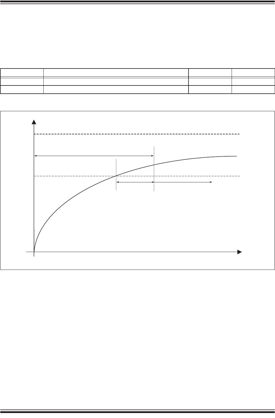
FIGURE 5-4: POWER-UP TIMING DIAGRAM
TABLE 5-8: RECOMMENDED SYSTEM POWER-UP TIMINGS
Symbol Parameter Minimum Units
T
PU-READ
1
1. This parameter is measured only for initial qualification and after a design or process change that could affect this parameter.
V
DD
Min to Read Operation 100 µs
T
PU-WRITE
1
V
DD
Min to Write Operation 100 µs
Time
V
DD
Min
V
DD
Max
V
DD
Device fully accessible
T
PU-READ
T
PU-WRITE
Chip selection is not allowed.
Commands may not be accepted or properly
interpreted by the device.
25137 PwrUp.0