SST25PF080B
DS20005137B-page 4 2014 Microchip Technology Inc.
3.0 MEMORY ORGANIZATION
The SST25PF080B SuperFlash memory array is orga-
nized in uniform 4 KByte erasable sectors with 32
KByte overlay blocks and 64 KByte overlay erasable
blocks.
4.0 DEVICE OPERATION
The SST25PF080B is accessed through the SPI (Serial
Peripheral Interface) bus compatible protocol. The SPI
bus consist of four control lines; Chip Enable (CE#) is
used to select the device, and data is accessed through
the Serial Data Input (SI), Serial Data Output (SO), and
Serial Clock (SCK).
The SST25PF080B supports both Mode 0 (0,0) and
Mode 3 (1,1) of SPI bus operations. The difference
between the two modes, as shown in Figure 4-1, is the
state of the SCK signal when the bus master is in
Standby mode and no data is being transferred. The
SCK signal is low for Mode 0 and SCK signal is high for
Mode 3. For both modes, the Serial Data In (SI) is sam-
pled at the rising edge of the SCK clock signal and the
Serial Data Output (SO) is driven after the falling edge
of the SCK clock signal.
FIGURE 4-1: SPI PROTOCOL
4.1 Hold Operation
The HOLD# pin is used to pause a serial sequence
underway with the SPI flash memory without resetting
the clocking sequence. To activate the HOLD# mode,
CE# must be in active low state. The HOLD# mode
begins when the SCK active low state coincides with
the falling edge of the HOLD# signal. The HOLD mode
ends when the HOLD# signal’s rising edge coincides
with the SCK active low state.
If the falling edge of the HOLD# signal does not coin-
cide with the SCK active low state, then the device
enters Hold mode when the SCK next reaches the
active low state. Similarly, if the rising edge of the
HOLD# signal does not coincide with the SCK active
low state, then the device exits in Hold mode when the
SCK next reaches the active low state. See Figure 4-2
for Hold Condition waveform.
Once the device enters Hold mode, SO will be in high-
impedance state while SI and SCK can be V
IL
or V
IH.
If CE# is driven active high during a Hold condition, the
device returns to Standby mode. As long as HOLD#
signal is low, the memory remains in the Hold condition.
To resume communication with the device, HOLD#
must be driven active high, and CE# must be driven
active low. See Figure 5-3 for Hold timing.
FIGURE 4-2: HOLD CONDITION WAVEFORM
25137 SPIprot.0
MODE 3
SCK
SI
SO
CE#
MODE 3
DON T CARE
Bit 7 Bit 6 Bit 5 Bit 4 Bit 3 Bit 2 Bit 1 Bit 0
MODE 0MODE 0
HIGH IMPEDANCE
MSB
MSB
Active Hold Active Hold Active
25137 HoldCond.0
SCK
HOLD#
2014 Microchip Technology Inc. DS20005137B-page 5
SST25PF080B
4.2 Write Protection
SST25PF080B provides software Write protection. The
Write Protect pin (WP#) enables or disables the lock-
down function of the status register. The Block-Protec-
tion bits (BP2, BP1, BP0, and BPL) in the status regis-
ter provide Write protection to the memory array and
the status register. See Table 4-3 for the Block-Protec-
tion description.
4.2.1 WRITE PROTECT PIN (WP#)
The Write Protect (WP#) pin enables the lock-down
function of the BPL bit (bit 7) in the status register.
When WP# is driven low, the execution of the Write-
Status-Register (WRSR) instruction is determined by
the value of the BPL bit (see Table 4-1). When WP# is
high, the lock-down function of the BPL bit is disabled.
4.3 Security ID
SST25PF080B offers a 256-bit Security ID (Sec ID)
feature. The Security ID space is divided into two parts
– one factory-programmed, 64-bit segment and one
user-programmable 192-bit segment. The factory-pro-
grammed segment is programmed at Microchip with a
unique number and cannot be changed. The user-pro-
grammable segment is left unprogrammed for the cus-
tomer to program as desired.
Use the Program SID command to program the Secu-
rity ID using the address shown in Table 4-5. Once pro-
grammed, the Security ID can be locked using the
Lockout SID command. This prevents any future write
to the Security ID.
The factory-programmed portion of the Security ID can
never be programmed, and none of the Security ID can
be erased.
4.4 Status Register
The software status register provides status on
whether the flash memory array is available for any
Read or Write operation, whether the device is Write
enabled, and the state of the Memory Write protection.
During an internal Erase or Program operation, the sta-
tus register may be read only to determine the comple-
tion of an operation in progress. Table 4-2 describes
the function of each bit in the software status register.
TABLE 4-1: CONDITIONS TO EXECUTE WRITE-STATUS-REGISTER (WRSR) INSTRUCTION
WP# BPL Execute WRSR Instruction
L1Not Allowed
L0Allowed
HXAllowed
TABLE 4-2: SOFTWARE STATUS REGISTER
Bit Name Function
Default at
Power-up Read/Write
0 BUSY 1 = Internal Write operation is in progress
0 = No internal Write operation is in progress
0R
1 WEL 1 = Device is memory Write enabled
0 = Device is not memory Write enabled
0R
2 BP0 Indicates current level of block write protection 1 R/W
3 BP1 Indicates current level of block write protection 1 R/W
4 BP2 Indicates current level of block write protection 1 R/W
5 SEC
1
1. The Security ID status will always be ‘1’ at power-up after a successful execution of the Lockout SID instruction; otherwise,
the default at power-up is ‘0’.
Security ID status
1 = Security ID space locked
0 = Security ID space not locked
0or1 R
6 AAI Auto Address Increment Programming status
1 = AII programming mode
0 = Byte-Program mode
0R
7 BPL 1 = BP2, BP1, BP0 are read-only bits
0 = BP2, BP1, BP0 are readable/writable
0 R/W
SST25PF080B
DS20005137B-page 6 2014 Microchip Technology Inc.
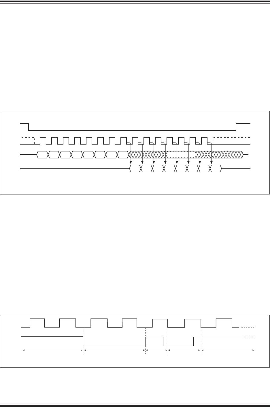
4.4.1 BUSY
The Busy bit determines whether there is an internal
Erase or Program operation in progress. A “1” for the
Busy bit indicates the device is busy with an operation
in progress. A “0” indicates the device is ready for the
next valid operation.
4.4.2 WRITE ENABLE LATCH (WEL)
The Write-Enable-Latch bit indicates the status of the
internal memory Write Enable Latch. If the Write-
Enable-Latch bit is set to “1”, it indicates the device is
Write enabled. If the bit is set to “0” (reset), it indicates
the device is not Write enabled and does not accept
any memory Write (Program/Erase) commands. The
Write-Enable-Latch bit is automatically reset under the
following conditions:
Power-up
Write-Disable (WRDI) instruction completion
Byte-Program instruction completion
Auto Address Increment (AAI) programming is
completed or reached its highest unprotected
memory address
Sector-Erase instruction completion
Block-Erase instruction completion
Chip-Erase instruction completion
Write-Status-Register instruction completion
Program SID instruction completion
Lockout SID instruction completion
4.4.3 AUTO ADDRESS INCREMENT (AAI)
The Auto Address Increment Programming-Status bit
provides status on whether the device is in AAI pro-
gramming mode or Byte-Program mode. The default at
power up is Byte-Program mode.
4.4.4 SECURITY ID STATUS (SEC)
The Security ID Status (SEC) bit indicates when the
Security ID space is locked to prevent a Write com-
mand. The SEC is ‘1’ after the host issues a Lockout
SID command. Once the host issues a Lockout SID
command, the SEC can never be reset to ‘0’.
4.4.5 BLOCK PROTECTION (BP2, BP1,
BP0)
The Block-Protection (BP2, BP1, BP0) bits define the
size of the memory area, as defined in Table 4-3, to be
software protected against any memory Write (Pro-
gram or Erase) operation. The Write-Status-Register
(WRSR) instruction is used to program the BP2, BP1
and BP0 bits as long as WP# is high or the Block-Pro-
tect-Lock (BPL) bit is 0. Chip-Erase can only be exe-
cuted if Block-Protection bits are all 0. After power-up,
BP2, BP1 and BP0 are set to 1.
4.4.6 BLOCK PROTECTION LOCK-DOWN
(BPL)
WP# pin driven low (V
IL
), enables the Block-Protection-
Lock-Down (BPL) bit. When BPL is set to 1, it prevents
any further alteration of the BPL, BP2, BP1, and BP0
bits. When the WP# pin is driven high (V
IH
), the BPL bit
has no effect and its value is “Don’t Care”. After power-
up, the BPL bit is reset to 0.
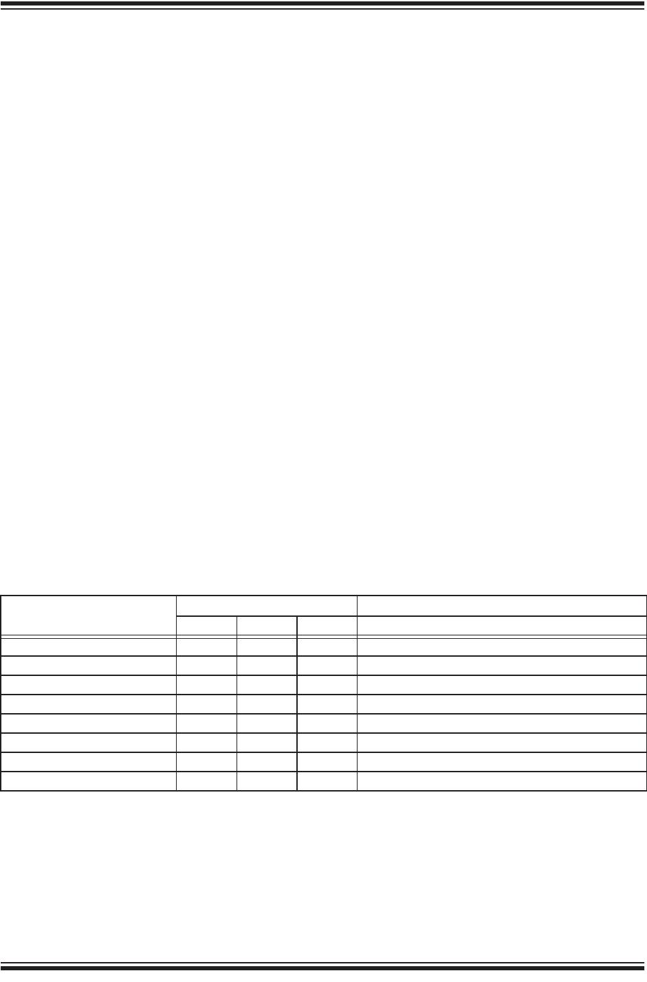
TABLE 4-3: SOFTWARE STATUS REGISTER BLOCK PROTECTION FOR SST25PF080B
1
1. X = Don’t Care (RESERVED) default is ‘0’
Protection Level
Status Register Bit
2
2. Default at power-up for BP2, BP1, and BP0 is ‘111’. (All Blocks Protected)
Protected Memory Address
BP2 BP1 BP0 8 Mbit
None 0 0 0 None
Upper 1/16 0 0 1 F0000H-FFFFFH
Upper 1/8 0 1 0 E0000H-FFFFFH
Upper 1/4 0 1 1 C0000H-FFFFFH
Upper 1/2 1 0 0 80000H-FFFFFH
All Blocks 1 0 1 00000H-FFFFFH
All Blocks 1 1 0 00000H-FFFFFH
All Blocks 1 1 1 00000H-FFFFFH

SST25PF080B-80-4C-QAE

Mfr. #:
Manufacturer:
Microchip Technology
Description:
NOR Flash 2.3V to 3.6V 8Mbit SPI Serial Flash
Lifecycle:
New from this manufacturer.
Delivery:
DHL FedEx Ups TNT EMS
Payment:
T/T Paypal Visa MoneyGram Western Union