‡Products and specifications discussed herein are for evaluation and reference purposes only and are subject to change by
Micron without notice. Products are only warranted by Micron to meet Micron’s production data sheet specifications.
152-Ball NAND Flash and Mobile LPDRAM PoP (TI OMAP) MCP
Features
Preliminary
‡
PDF: 09005aef8326e5ac / Source: 09005aef8326e59a Micron Technology, Inc., reserves the right to change products or specifications without notice.
152ball_ nand_lpdram_j4xx_omap.fm - Rev. E 4/09 EN
1 ©2008 Micron Technology, Inc. All rights reserved.
NAND Flash and Mobile LPDRAM
152-Ball Package-on-Package (PoP)
Combination Memory (TI OMAP™)
MT29C Family
Current production part numbers: See Table 1 on page 3
Features
•Micron
®
NAND Flash and Mobile LPDRAM
components
• RoHS-compliant, “green” package
• Separate NAND Flash and Mobile LPDRAM
interfaces
• Space-saving package-on-package combination
• Low-voltage operation (1.70–1.95V)
• Industrial temperature range: –40°C to +85°C
NAND Flash-Specific Features
• Organization
– Page size
x8: 2112 bytes (2048 + 64 bytes)
x16: 1056 words (1024 + 32 words)
– Block size: 64 pages (128K + 4K bytes)
Mobile LPDRAM-Specific Features
• No external voltage reference required
• No minimum clock rate requirement
• 1.8V LVCMOS-compatible inputs
• Programmable burst lengths
• Partial-array self refresh (PASR)
• Deep power-down (DPD) mode
• Selectable output drive strength
• STATUS REGISTER READ (SRR) supported
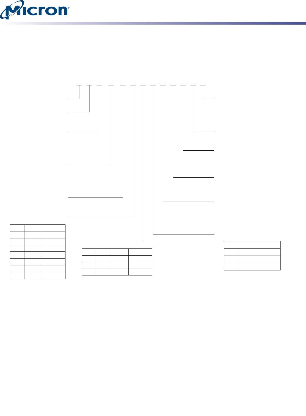
1
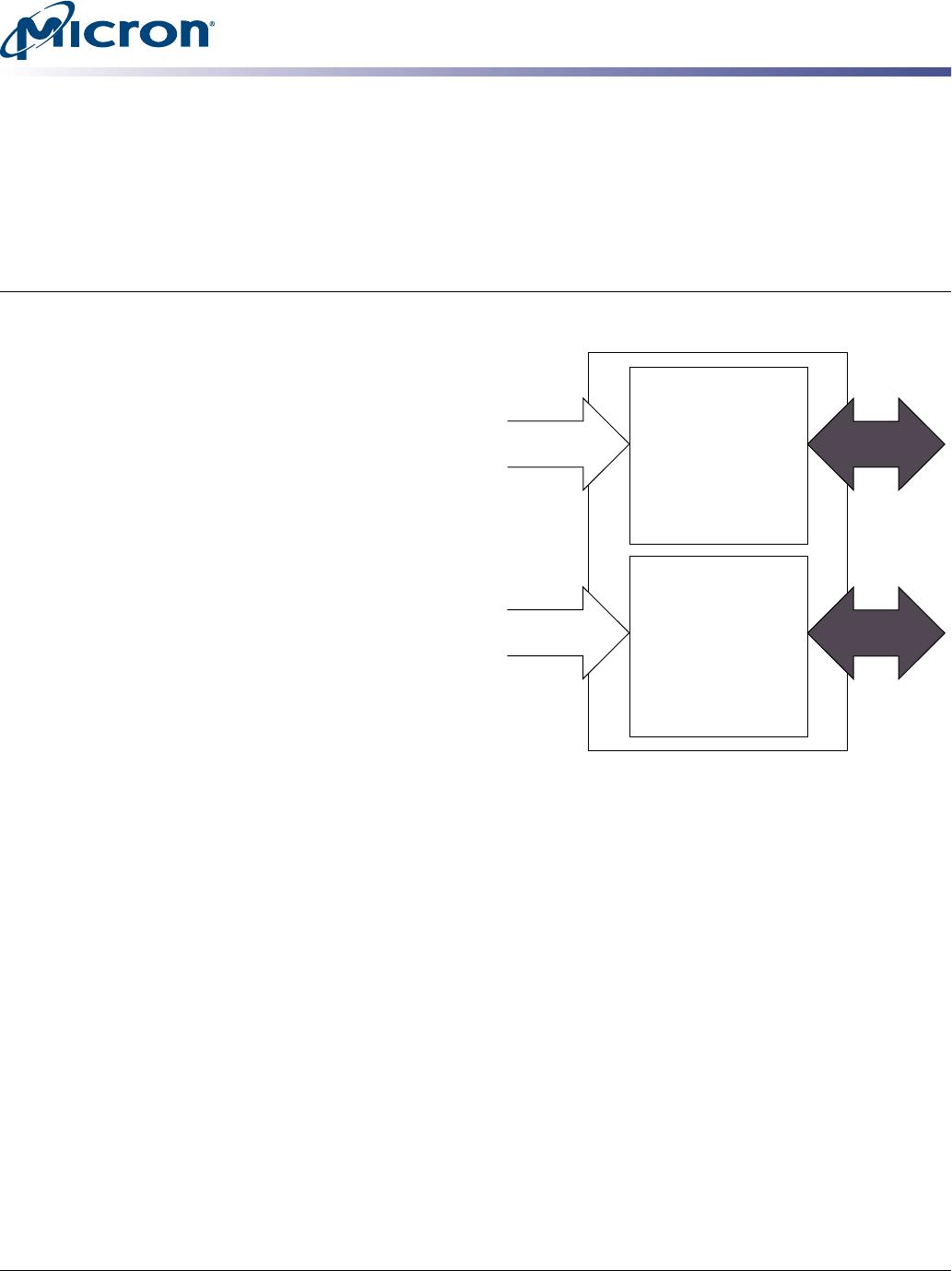
Figure 1: PoP Block Diagram
Notes: 1. Contact factory for remapped SRR output.
2. CL = CAS (READ) latency.
Options Marking
•LP-DRAM
166 MHz CL3
2
-6
133 MHz CL3
-75
NAND Flash
Device
NAND Flash
Power
NAND Flash
Interface
LP-DRAM Power
LP-DRAM Interface
LP-DRAM
Device