MT29C2G24MAABAKAMD-5 IT

PDF: 09005aef8326e5ac / Source: 09005aef8326e59a Micron Technology, Inc., reserves the right to change products or specifications without notice.
152ball_ nand_lpdram_j4xx_omap.fm - Rev. E 4/09 EN
7 ©2008 Micron Technology, Inc. All rights reserved.
152-Ball NAND Flash and Mobile LPDRAM PoP (TI OMAP) MCP
Ball Assignments and Descriptions
Preliminary
Notes: 1. Balls marked RFU may or may not be connected internally. These balls should not be used.
Contact the factory for details.
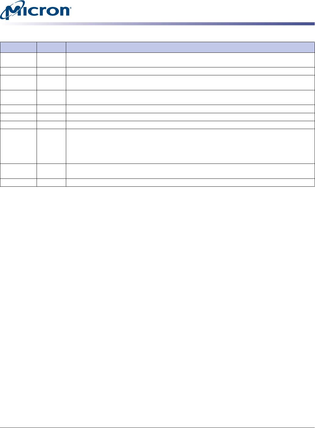
Table 2: x8/x16 NAND Ball Descriptions
Symbol Type Description
ALE Input
Address latch enable: When ALE is HIGH, addresses can be transferred to the on-chip address
register.
CE1#, CE0# Input
Chip enable: Gates transfers between the host system and the NAND Flash device.
CLE Input
Command latch enable: When CLE is HIGH, commands can be transferred to the on-chip
command register.
LOCK Input
When LOCK is HIGH during power-up, the BLOCK LOCK function is enabled. To disable BLOCK
LOCK, connect LOCK to V
SS
during power-up, or leave it unconnected (internal pull-down).
RE# Input
Read enable: Gates information from the NAND device to the host system.
WE# Input
Write enable: Gates information from the host system to the NAND device.
WP# Input
Write protect: Driving WP# LOW blocks ERASE and PROGRAM operations.
I/O[7:0]
(x8)
I/O[15:0]
(x16)
Input/
output
Data inputs/outputs: The bidirectional I/Os transfer address, data, and instruction information.
Data is output only during READ operations; at other times the I/Os are inputs.
I/O[15:8] are RFU
1
for NAND x8 devices.
R/B# Output
Ready/busy: Open-drain, active-LOW output that indicates when an internal operation is in
progress.
V
CC
Supply
V
CC
: NAND power supply.
PDF: 09005aef8326e5ac / Source: 09005aef8326e59a Micron Technology, Inc., reserves the right to change products or specifications without notice.
152ball_ nand_lpdram_j4xx_omap.fm - Rev. E 4/09 EN
8 ©2008 Micron Technology, Inc. All rights reserved.
152-Ball NAND Flash and Mobile LPDRAM PoP (TI OMAP) MCP
Ball Assignments and Descriptions
Preliminary
Notes: 1. Balls marked RFU may or may not be connected internally. These balls should not be used.
Contact the factory for details.
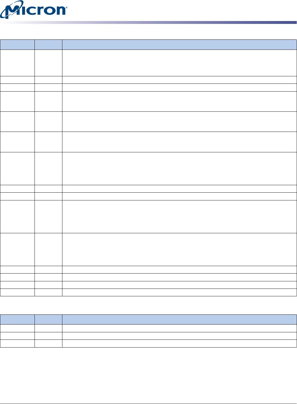
Table 3: x16/x32 LPDDR Ball Descriptions
Symbol Type Description
A[14:0] Input
Address inputs: Specifies the row or column address. Also used to load the mode registers. The
maximum LPDDR address is determined by density and configuration. Consult the LPDDR
product data sheet for the maximum address for a given density and configuration. Unused
address pins become RFU.
BA1, BA0 Input
Bank address inputs: Specifies one of the 4 banks.
CAS# Input
Column select: Specifies the command to execute.
CK, CK# Input
CK is the system clock. CK and CK# are differential clock inputs. All address and control signals
are sampled and referenced on the crossing of the rising edge of CK with the falling edge of
CK#.
CKE0, CKE1 Input
Clock enable:
CKE0 is used for a single LPDDR product.
CKE1 is used for dual LPDDR products.
CS1#, CS0# Input
Chip select:
CS0# is used for a single LPDDR product.
CS1# is used for dual LPDDR products and is considered RFU for single LPDDR MCPs.
LDM, UDM
(x16)
DM[3:0]
(x32)
Input
Data mask: Determines which bytes are written during WRITE operations.
For x16 LPDDR, unused DM balls become RFU.
RAS# Input
Row select: Specifies the command to execute.
WE# Input
Write enable: Specifies the command to execute.
DQ[15:0]
(x16)
DQ[31:0]
(x32)
Input/
output
Data bus: Data inputs/outputs.
DQ[31:16] are RFU for x16 LPDDR devices.
LDQS, UDQS
(x16)
DQS[3:0]
(x32)
Input/
output
Data strobe: Coordinates READ/WRITE transfers of data; one DQS per DQ byte.
For x16 LPDDR, unused DQS balls become RFU.
TQ Output
Temperature sensor output: TQ HIGH when LPDDR T
J
exceeds 85°C.
V
DD
Supply
V
DD
: LPDDR power supply.
V
DDQ
Supply
V
DDQ
: LPDDR I/O power supply.
V
SSQ
Supply
V
SSQ
: LPDDR I/O ground.
Table 4: Non-Device-Specific Ball Descriptions
Symbol Type Description
V
SS
Supply
V
SS
: Shared ground.
NC
No connect: Not internally connected.
RFU
1
Reserved for future use.
PDF: 09005aef8326e5ac / Source: 09005aef8326e59a Micron Technology, Inc., reserves the right to change products or specifications without notice.
152ball_ nand_lpdram_j4xx_omap.fm - Rev. E 4/09 EN
9 ©2008 Micron Technology, Inc. All rights reserved.
152-Ball NAND Flash and Mobile LPDRAM PoP (TI OMAP) MCP
Electrical Specifications
Preliminary
Electrical Specifications
Notes: 1. Supply voltage references either V
CC
,V
DD
, or V
DDQ
.
Stresses greater than those listed under “Absolute Maximum Ratings” may cause perma-
nent damage to the device. This is a stress rating only, and functional operation of the
device at these or any other conditions above those indicated in the operational sections
of this specification is not implied. Exposure to absolute maximum rating conditions for
extended periods may affect reliability.
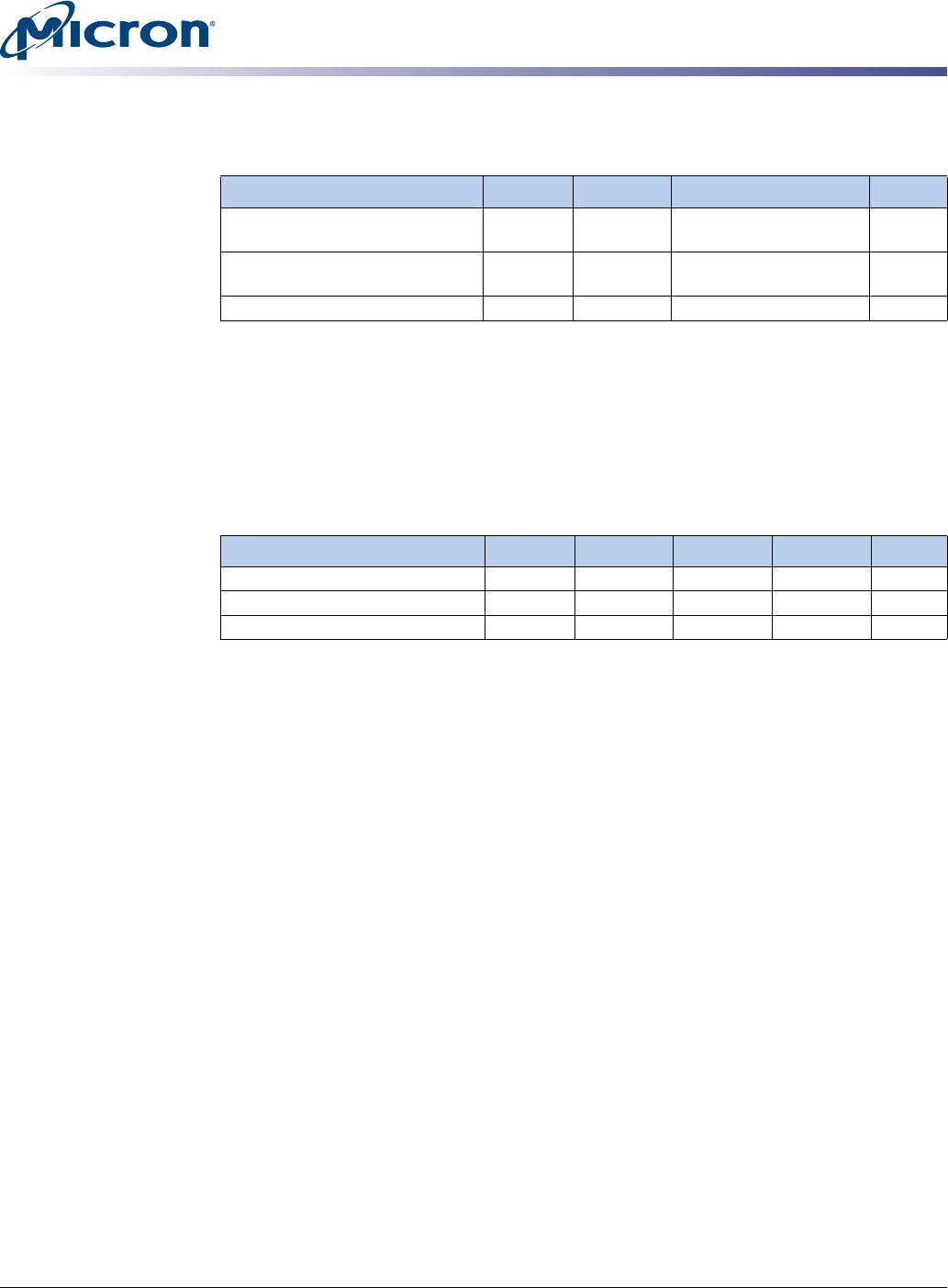
Table 5: Absolute Maximum Ratings
Parameters/Conditions Symbol Min Max Unit
V
CC
, V
DD
, V
DDQ
Supply voltage
relative to V
SS
V
CC
, V
DD
,
V
DDQ
–1.0 2.4 V
Voltage on any pin
relative to V
SS
V
IN
–0.5 2.4 or (supply voltage
1
+
0.3V), whichever is less
V
Storage temperature range
–55 +150 °C
Table 6: Recommended Operating Conditions
Parameters Symbol Min Typ Max Unit
Supply voltage
V
CC
, V
DD
1.70 1.80 1.95 V
I/O supply voltage
V
DDQ
1.70 1.80 1.95 V
Operating temperature range
–40 +85 °C

MT29C2G24MAABAKAMD-5 IT

Mfr. #:
Manufacturer:
Micron
Description:
IC FLASH RAM 2G PARAL 130VFBGA
Lifecycle:
New from this manufacturer.
Delivery:
DHL FedEx Ups TNT EMS
Payment:
T/T Paypal Visa MoneyGram Western Union