SS8P2CL, SS8P3CL
www.vishay.com
Vishay General Semiconductor
Revision: 10-Dec-14
1
Document Number: 89030
For technical questions within your region: DiodesAmericas@vishay.com
, DiodesAsia@vishay.com, DiodesEurope@vishay.com
THIS DOCUMENT IS SUBJECT TO CHANGE WITHOUT NOTICE. THE PRODUCTS DESCRIBED HEREIN AND THIS DOCUMENT
ARE SUBJECT TO SPECIFIC DISCLAIMERS, SET FORTH AT www.vishay.com/doc?91000
High Current Density Surface Mount
Schottky Barrier Rectifier
FEATURES
• Very low profile - typical height of 1.1 mm
• Ideal for automated placement
• Low forward voltage drop, low power losses
• High efficiency
• Low thermal resistance
• Meets MSL level 1, per J-STD-020
• AEC-Q101 qualified available
- Automotive ordering code: base P/NHM3
• Material categorization: for definitions of compliance
please see www.vishay.com/doc?99912
TYPICAL APPLICATIONS
For use in low voltage high frequency inverters, freewheeling
diodes, DC/DC converters, and polarity protection
application.
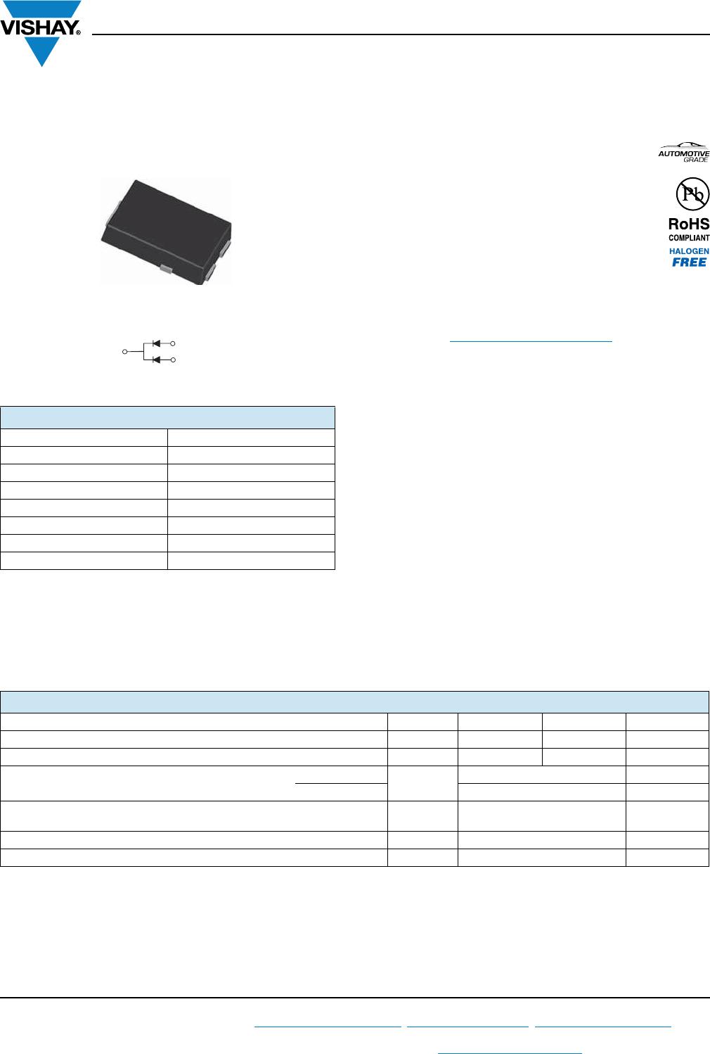
MECHANICAL DATA
Case: TO-277A (SMPC)
Molding compound meets UL 94 V-0 flammability rating
Base P/N-M3 - halogen-free, RoHS-compliant, and
commercial grade
Base P/NHM3 - halogen-free, RoHS-compliant and
AEC-Q101 qualified
Base P/NHM3_X - halogen-free, RoHS-compliant and
AEC-Q101 qualified
(“_X” denotes revision code e.g. A, B,.....)
Terminals: Matte tin plated leads, solderable per
J-STD-002 and JESD 22-B102
M3 suffix meets JESD 201 class 2 whisker test, HM3 suffix
meets JESD 201 class 2 whisker test
PRIMARY CHARACTERISTICS
I
F(AV)
2 x 4.0 A
V
RRM
20 V, 30 V
I
FSM
120 A
E
AS
20 mJ
V
F
at I
F
= 4 A 0.41 V
T
J
max. 150 °C
Package TO-277A
Diode variations Single
TO-277A (SMPC)
K
2
1
Anode 1
Anode 2
Cathode
K
eSMP
®
Series
Available
MAXIMUM RATINGS (T
A
= 25 °C unless otherwise noted)
PARAMETER SYMBOL SS8P2CL SS8P3CL UNIT
Device marking code S82C S83C
Maximum repetitive peak reverse voltage V
RRM
20 30 V
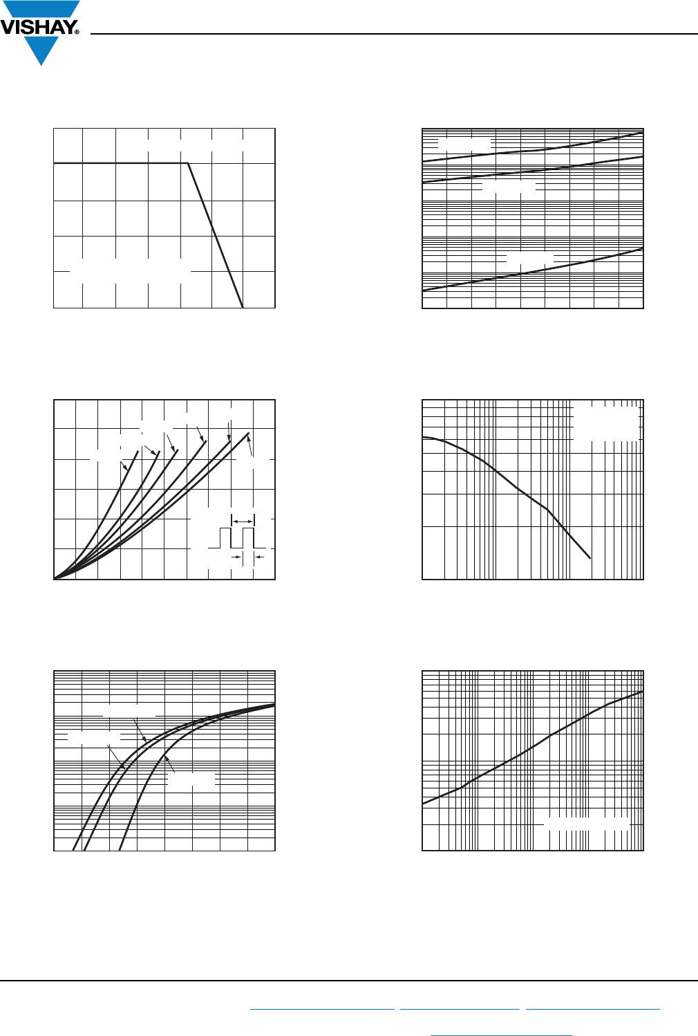
Maximum average forward rectified current (fig. 1)
total device
I
F(AV)
8.0 A
per diode 4.0
Peak forward surge current 10 ms single half sine-wave
superimposed on rated load
I
FSM
120 A
Non-repetitive avalanche energy at 25 °C, I
AS
= 2 A per diode E
AS
20 mJ
Operating junction and storage temperature range T
J
, T
STG
-55 to +150 °C