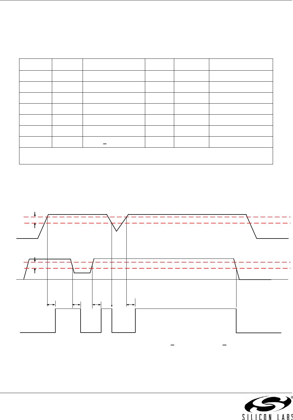
Si8220/21
Rev. 1.2 13
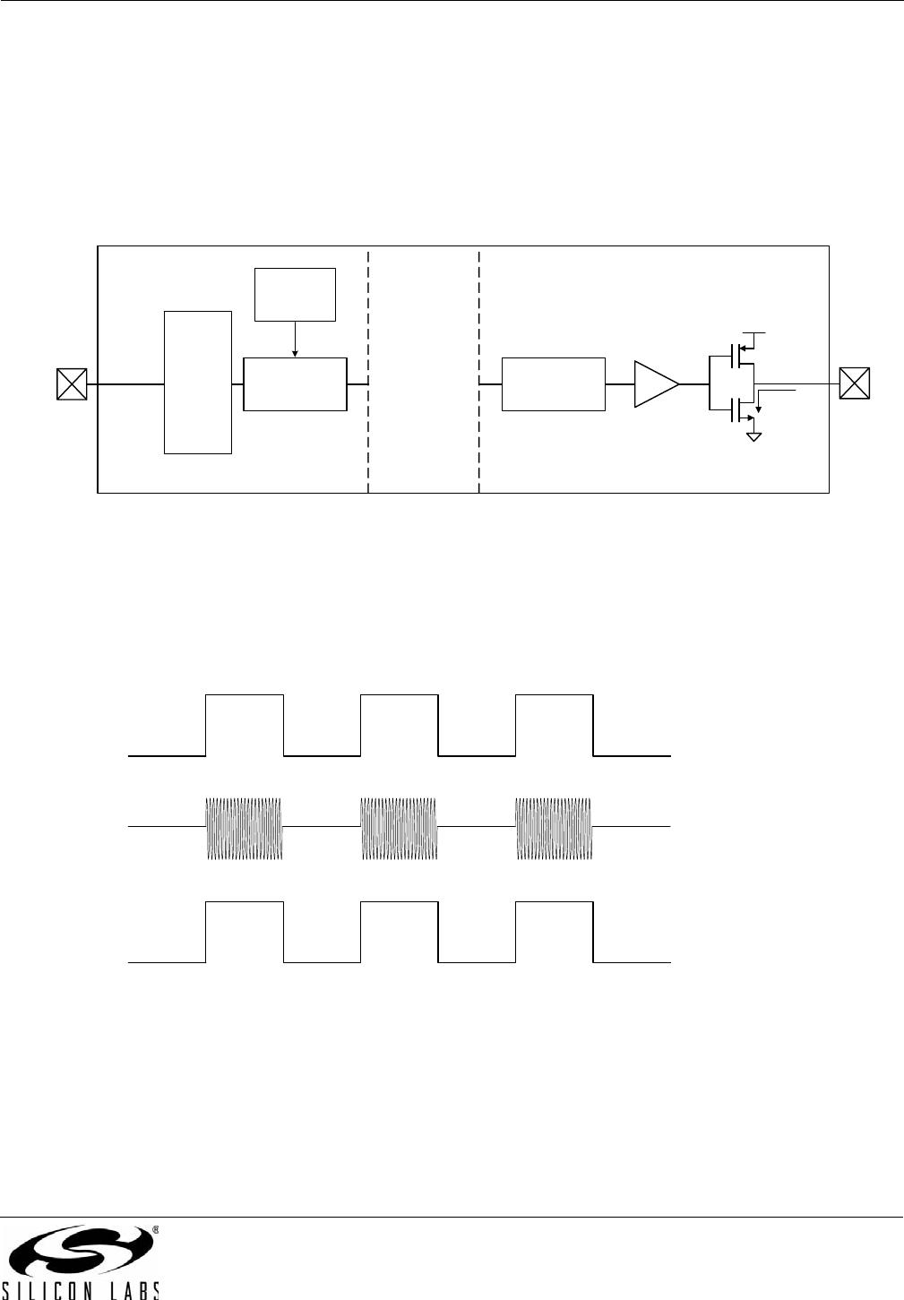
4. Functional Description
4.1. Theory of Operation
The Si8220/21 is a functional upgrade for popular opto-isolated drivers, such as the Avago HPCL-3120, HPCL-
0302, Toshiba TLP350, and others. The operation of an Si8220/21 channel is analogous to that of an opto coupler,
except an RF carrier is modulated instead of light. This simple architecture provides a robust isolated data path and
requires no special considerations or initialization at start-up. A simplified block diagram for the Si8220/21 is shown
in Figure 6.
Figure 6. Simplified Channel Diagram
A channel consists of an RF Transmitter and RF Receiver separated by a semiconductor-based isolation barrier.
Referring to the Transmitter, input A modulates the carrier provided by an RF oscillator using on/off keying. The
Receiver contains a demodulator that decodes the input state according to its RF energy content and applies the
result to output B via the output driver. This RF on/off keying scheme is superior to pulse code schemes as it
provides best-in-class noise immunity, low power consumption, and better immunity to magnetic fields. See
Figure 7 for more details.
Figure 7. Modulation Scheme
RF
OSCILLATOR
MODULATOR DEMODULATOR
A
B
Semiconductor-
Based Isolation
Barrier
Transmitter
Receiver
LED
Emulator
0.5 to 2.5 A
peak
Gnd
V
DD
Input Signal
Output Signal
Modulation Signal
Si8220/21
14 Rev. 1.2
5. Technical Description
5.1. Device Behavior
Truth tables for the Si8220/21 are summarized in Table 9.
5.2. Device Startup
Output V
O
is held low during power-up until V
DD
rises above the UVLO+ threshold for a minimum time period of
t
START
. Following this, the output is high when the current flowing from anode to cathode is > I
F(ON)
. Device startup,
normal operation, and shutdown behavior is shown in Figure 8.
Figure 8. Si8220/21 Operating Behavior (I
F
> I
F(MIN)
when V
F
> V
F(MIN)
)
Table 9. Si8220/21 Truth Table Summary
Cathode Anode Diode Current (I
F
)V
DD
VO Comments
X X X < UVLO L Device turned off
Hi-Z X 0 > UVLO L Logic low state
X Hi-Z 0 > UVLO L Logic low state
GND GND 0 > UVLO L Logic low state
VF VF 0 > UVLO L Logic low state
GND1 VF < I
F(OFF
> UVLO L Logic low state
GND1 VF >
I
F(OFF)
> UVLO H Logic high state
Note: “X” = don’t care. This truth table assumes VDD is powered. If VDD is below UVLO, see "5.3.Under
Voltage Lockout (UVLO)" on page 15 for more information.
I
F
V
O
V
DD
t
START
t
START
V
DDHYS
t
PHL
t
PLH
I
F(ON)
UVLO+
UVLO-
I
HYS
Si8220/21
Rev. 1.2 15
5.3. Under Voltage Lockout (UVLO)
The UVLO circuit unconditionally drives V
O
low when V
DD
is below the lockout threshold. Referring to Figures 9
through 12, upon power up, the Si8220/21 is maintained in UVLO until VDD rises above VDD
UV+
. During power
down, the Si8220/21 enters UVLO when VDD falls below the UVLO threshold plus hysteresis (i.e., VDD <
VDD
UV+
– VDD
HYS
).
Figure 9. Si8220/21 UVLO Response (5 V)
Figure 10. Si8220/21 UVLO Response (8 V)
Figure 11. Si8220/21 UVLO Response (10 V)
Figure 12. Si8220/21 UVLO Response (12.5 V)
3.5
10.5
V
DDUV+
(Typ)
Output Voltage (V
O
)
4.0 4.5 5.0 5.5 6.0 6.5 7.0 7.5
Supply Voltage (V
DD
- V
SS
) (V)
6.0
10.5
V
DDUV+
(Typ)
Output Voltage (V
O
)
6.5 7.0 7.5 8.0 8.5 9.0 9.5 10.0
Supply Voltage (V
DD
- V
SS
) (V)
8.5
10.5
V
DDUV+
(Typ)
Output Voltage (V
O
)
9.0 9.5 10.0 10.5 11.0 11.5 12.0 12.5
Supply Voltage (V
DD
- V
SS
) (V)
11.3
10.5
V
DDUV+
(Typ)
Output Voltage (V
O
)
11.8 12.3 12.8 13.3 13.8 14.3 14.8 15.3
Supply Voltage (V
DD
- V
SS
) (V)

SI8220BD-D-ISR

Mfr. #:
Manufacturer:
Silicon Labs
Description:
Gate Drivers 5 kV opto input isolated gate driver
Lifecycle:
New from this manufacturer.
Delivery:
DHL FedEx Ups TNT EMS
Payment:
T/T Paypal Visa MoneyGram Western Union