Si8220/21
16 Rev. 1.2
6. Applications
6.1. Power Supply Connections
V
SS
can be biased at, above, or below ground as long as the voltage on V
DD
with respect to V
SS
is a maximum of
24 V. V
DD
decoupling capacitors should be placed as close to the package pins as possible. The optimum values
for these capacitors depend on load current and the distance between the chip and its power source. It is
recommended that 0.1 and 10 µF bypass capacitors be used to reduce high-frequency noise and maximize
performance.
6.2. Layout Considerations
It is most important to minimize ringing in the drive path and noise on the V
DD
lines. Care must be taken to
minimize parasitic inductance in these paths by locating the Si8220/21 as close to the device it is driving as
possible. In addition, the V
DD
supply and ground trace paths must be kept short. For this reason, the use of power
and ground planes is highly recommended. A split ground plane system having separate ground and V
DD
planes
for power devices and small signal components provides the best overall noise performance.
6.3. Power Dissipation Considerations
Proper system design must assure that the Si8220/21 operates within safe thermal limits across the entire load
range. The Si8220/21 total power dissipation is the sum of the power dissipated by bias supply current, internal
switching losses, and power delivered to the load, as shown in Equation 1.
Equation 1.
The maximum allowable power dissipation for the Si8220/21 is a function of the package thermal resistance,
ambient temperature, and maximum allowable junction temperature, as shown in Equation 2.
Equation 2.
Substituting values for P
Dmax
T
jmax
, T
A
, and
ja
into Equation 2 results in a maximum allowable total power
dissipation of 1.0 W. The maximum allowable load is found by substituting this limit and the appropriate datasheet
values from Table 1 on page 4 into Equation 1 and simplifying. The result is Equation 3, where V
F
=2.8V,
I
F
= 10 mA, and V
DD
=18V.
P
D
V
F
I
F
Duty CycleV
DD
I
QOUT
C
int
V
DD
2
F C
L
V
DD
2
F
where:
P
D
is the total Si8220 device power dissipation (W)
I
F
is the diode current (20 mA max)
V
F
is the diode anode voltage (2.8 V max)
I
QOUT
is the driver maximum bias curent (5 mA)
C
int
is the internal parasitic capacitance (370 pF)
V
DD
is the driver-side supply voltage (24 V max)
F is the switching frequency (Hz)
++ +=
P
Dmax
T
jmax
T
A
ja
---------------------------
where:
P
Dmax
is the maximum allowable Si8220/21 power dissipation (W)
T
jmax
is the Si8220/21 maximum junction temperature (150 °C)
T
A
is the ambient temperature (°C)
ja
is the Si8220/21 package junction-to-air thermal resistance (125 °C/W)
Si8220/21
Rev. 1.2 17
Equation 3.
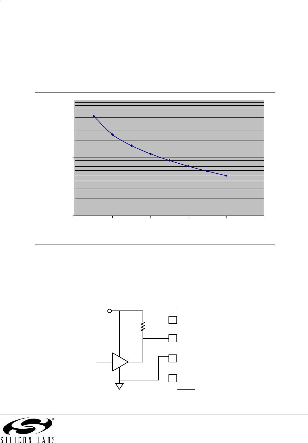
A graph of Equation 3 is shown in Figure 13. Each point along the load line in this graph represents the package
dissipation-limited value of C
L
for the corresponding switching frequency.
Figure 13. Maximum Load vs. Switching Frequency
6.4. Input Circuit Design
Opto driver manufacturers typically recommend the circuits shown in Figures 14 and 15. These circuits are
specifically designed to improve opto-coupler input common-mode rejection and increase noise immunity.
Figure 14. Opto Driver Input Circuit
C
Lmax
1.35 10
3
F
------------------------------
1.85 10
10
where:
C
Lmax
is the maximum load (pF) allowable at switching frequency F
=
100
1,000
10,000
0 500 1,000 1,500 2,000 2,500
Frequency (KHz)
Load (pF)
R1
1
2
3
4
OPTO DRIVER
Vdd
Open Drain or
Collector
Control
Input
ANODE
CATHODE
N/C
N/C
Si8220/21
18 Rev. 1.2
Figure 15. High CMR Opto Driver Input Circuit
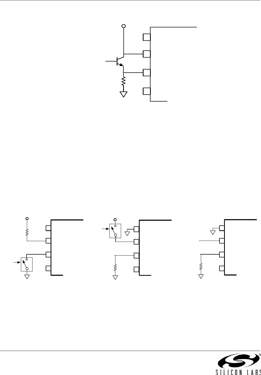
The optically-coupled driver circuit of Figure 14 turns the LED on when the control input is high. However, internal
capacitive coupling from the LED to the power and ground conductors can momentarily force the LED into its off
state when the anode and cathode inputs are subjected to a high common-mode transient. The circuit shown in
Figure 15 addresses this issue by using a value of R1 sufficiently low to overdrive the LED, ensuring it remains on
during an input common-mode transient. Q1 shorts the LED off in the low output state, again increasing common-
mode transient immunity. Some opto driver applications also recommend reverse-biasing the LED when the
control input is off to prevent coupled noise from energizing the LED.
The Si8220/21 can be used with the input circuits shown in Figures 14 and 15; however, some applications will
require increasing the value of R1 in order to limit I
F
to a maximum of 20 mA. The Si8220/21 propagation delay and
output drive do not change for values of I
F
between I
F(MIN)
and I
F(MAX)
. New designs should consider the input
circuit configurations of Figure 16, which are more efficient than those of Figures 14 and 15. As shown, S1
represents any suitable switch, such as a BJT or MOSFET, analog transmission gate, processor I/O, etc. Also, note
that the Si8220/21 input can be driven from the I/O port of any MCU or FPGA capable of sourcing a minimum of
5 mA (see Figure 16C).
Figure 16. Si8220/21 Other Input Circuit Configurations
R1
1
2
3
4
OPTO DRIVER
Vdd
Control
Input
ANODE
CATHODE
N/C
N/C
Q1
1
2
3
4
Control
Input
+5V
R1
S1
Si8220/21
N/C
ANODE
CATHODE
N/C
See Text
Si8220/21
1
2
3
4
+5V
R1
Control
Input
S1
N/C
ANODE
CATHODE
N/C
See Text
1
2
3
4
R1
MCU I/O
Port pin
Si8220/21
N/C
ANODE
CATHODE
N/C
A
B
C

SI8220BD-D-ISR

Mfr. #:
Manufacturer:
Silicon Labs
Description:
Gate Drivers 5 kV opto input isolated gate driver
Lifecycle:
New from this manufacturer.
Delivery:
DHL FedEx Ups TNT EMS
Payment:
T/T Paypal Visa MoneyGram Western Union