Expand menu
Hello, Sign in
My Account
0
Cart
Home
Products
Sensors
Semiconductors
Passive Components
Connectors
Power
Electromechanical
Optoelectronics
Circuit Protection
Integrated Circuits - ICs
Main Products
Manufacturers
Blog
Services
About OMO
About Us
Contact Us
Check Stock
SI8220BD-D-ISR
P1-P3
P4-P6
P7-P9
P10-P12
P13-P15
P16-P18
P19-P21
P22-P24
P25-P27
P28-P30
P31-P32
Si8220/21
Rev. 1.2
25
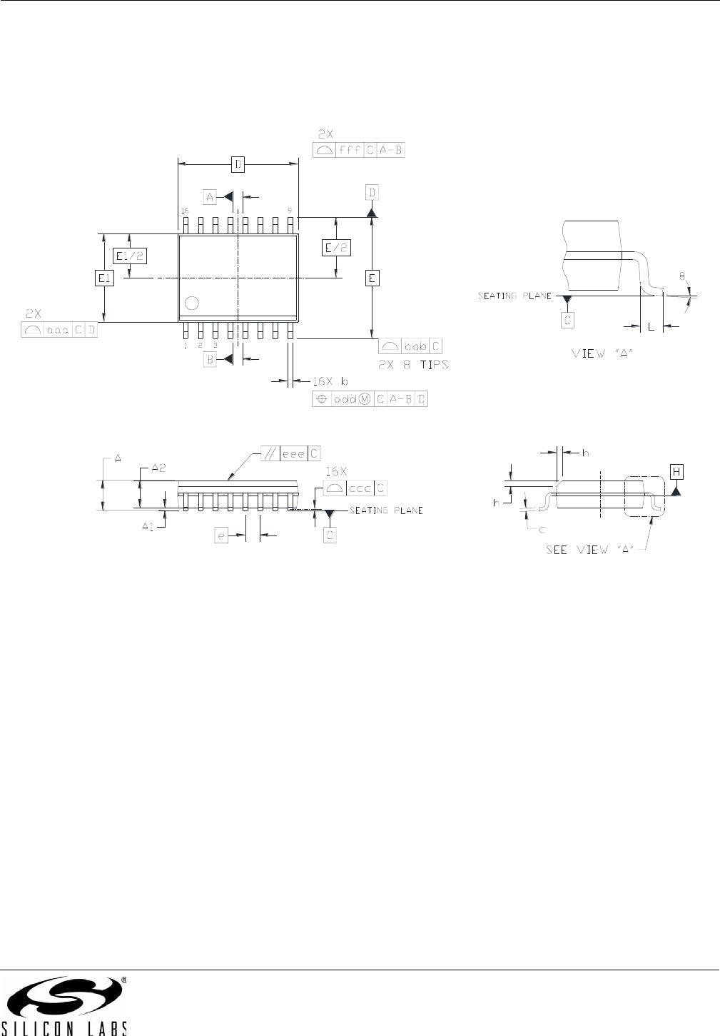
12. Package Outline:
16-Pin Wide Body SOIC
Figure 20 illustrates the p
a
ckage
details for the Si822x Digit
al Isolator
. T
a
ble 17 list
s the values for the dimensions
shown in the illustration.
Figure 20. 16-Pin Wide
Body SOIC
Si8220/21
26
Rev. 1.2
T
able 17. Package Diagram Dimension
s
Dimension
Min
Max
A
—
2.65
A1
0.10
0.30
A2
2.05
—
b
0.31
0.51
c
0.20
0.33
D
10.30 BSC
E
1
0.30 BSC
E1
7.50 BSC
e
1.27 BSC
L
0.40
1.27
h
0.25
0.75
0°
8°
aaa
—0
.
1
0
bbb
—
0.33
ccc
—
0.10
ddd
—
0.25
eee
—
0.10
fff
—
0.20
Notes:
1.
All dimensions shown are in mil
limeters (mm) unless otherwise noted.
2.
Dimensioning and T
olerancing p
er ANSI Y14.5M-1994.
3.
This drawing conforms to JEDEC Outline MS-013, V
ariation AA.
4.
Recommended reflow profile
per JEDE
C J-STD-0
20C specification for
small body
, lead-free componen
ts.
Si8220/21
Rev. 1.2
27
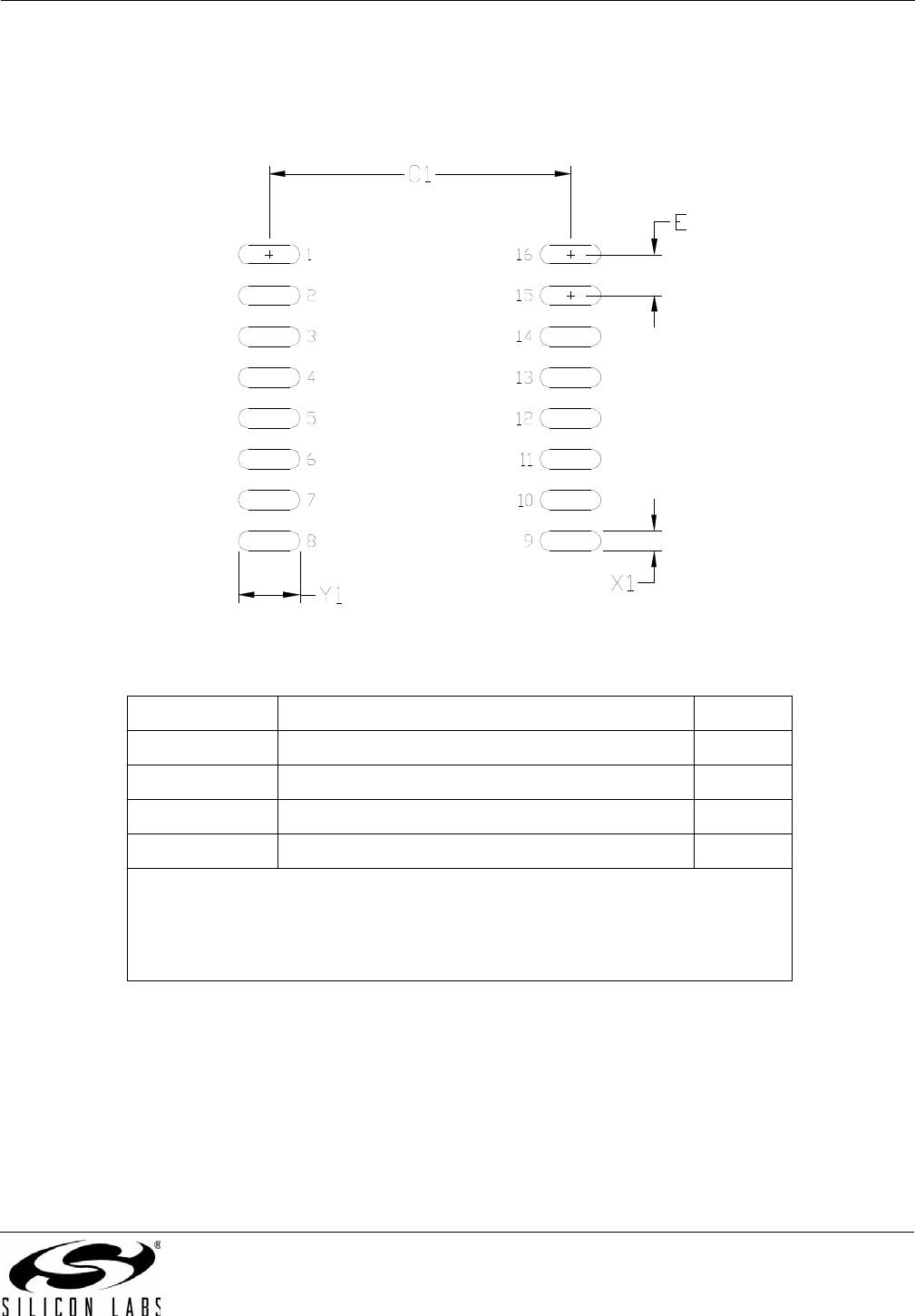
13. Land Pattern: 16-Pin Wide-Body SOIC
Figure
21
illustrates the reco
mmended land pattern det
ails
for the Si822x in a 16-p
in wide-body SOIC. T
able
18
lists the values for the dimens
ions shown in the illustration.
Figure 21. 16-Pi
n SOIC Land Pattern
T
able 18. 16-Pin Wide Bod
y SOIC Land Pattern Dimensions
Dimension
Feature
(mm)
C1
Pad Column S
pacing
9.40
E
Pad Row Pitch
1.27
X1
P
ad Wid
th
0.60
Y1
Pad Length
1.90
Notes:
1.
This Land Pattern Design is based o
n IPC-7351 pattern SOIC127P1032X265-16AN
for Density Level B (Median Land Pro
trusion).
2.
All feature sizes shown are at Maximum Material Condition (MMC) and a card
fabrication tolerance of 0.05 mm is assumed.
P1-P3
P4-P6
P7-P9
P10-P12
P13-P15
P16-P18
P19-P21
P22-P24
P25-P27
P28-P30
P31-P32
SI8220BD-D-ISR
Mfr. #:
Buy SI8220BD-D-ISR
Manufacturer:
Silicon Labs
Description:
Gate Drivers 5 kV opto input isolated gate driver
Lifecycle:
New from this manufacturer.
Delivery:
DHL
FedEx
Ups
TNT
EMS
Payment:
T/T
Paypal
Visa
MoneyGram
Western
Union
Products related to this Datasheet
SI8220DB-D-IS
SI8220BB-D-IS
SI8220BB-D-ISR
SI8220CB-D-IS
SI8220DD-D-IS
SI8220BD-D-IS
SI8221CC-D-IS
SI8221DC-D-IS
SI8220DB-D-ISR
SI8221DC-D-ISR
SI8221CC-D-ISR
SI8220BD-D-ISR
SI8220DD-D-ISR
SI8220CB-D-ISR
SI8220DB-A-IS
SI8220DD-A-IS
SI8221CC-A-IS
SI8220CB-A-ISR
SI8220DB-A-ISR
SI8220BB-A-IS
SI8220CD-A-ISR
SI8220BB-A-ISR
SI8220BD-A-IS
SI8220BD-A-ISR
SI8220CB-A-IS
SI8220CD-A-IS
SI8220DD-A-ISR
SI8221CC-A-ISR
SI8221DC-A-IS
SI8221DC-A-ISR