LTC4231
7
4321fa
For more information www.linear.com/LTC4231
pin FuncTions
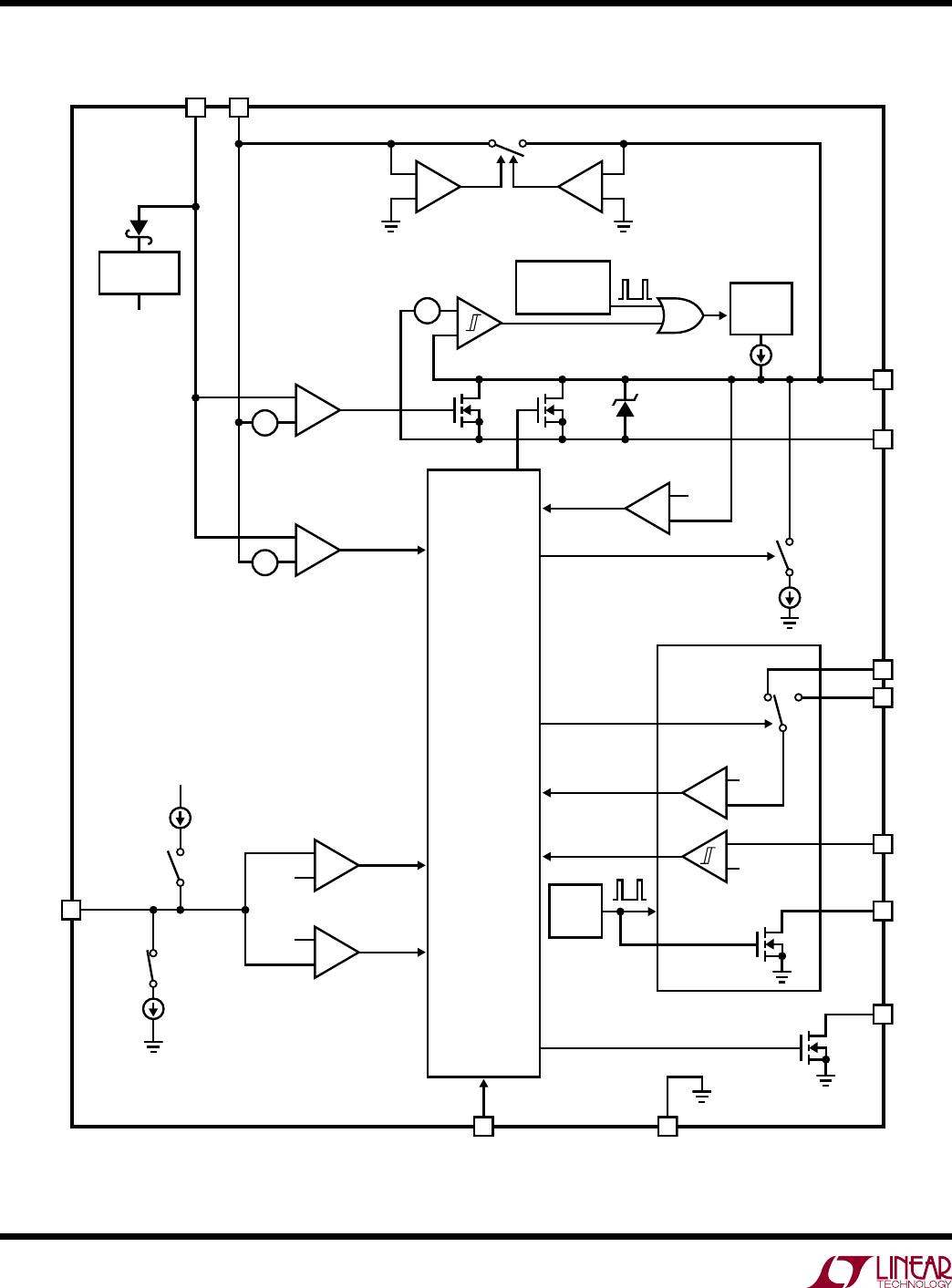
GATE: Gate Drive for External N-Channel MOSFET. After
all start-up conditions are satisfied, a 10μA pull-up cur-
rent from
the internal charge pump charges up
∆V
GATE
to
the high threshold voltage ∆V
GATE(H)
and then turns off.
The charge pump turns on again when ∆V
GATE
decays by
more than 0.7V or every 15ms, whichever comes first,
and recharges ∆V
GATE
to ∆V
GATE(H)
. During GATE turn-
off, a 1mA pull-down current discharges GATE to GND.
During severe short circuits, a 130mA pull-down current
is activated to discharge GATE to SOURCE.
GND: Device Ground.
GNDSW: Switched GND. Connect this pin to an external
resistive network to monitor IN for overvoltage or under
-
voltage (OV/UV). To reduce
the power dissipated by this
resistive divider, the LTC4231 periodically samples IN by
connecting GNDSW to GND once every 10ms. Tie this pin
to GND if unused.
IN: Supply Voltage and Current Sense Input. This pin has
a nominal undervoltage lockout threshold of 2.3V.
SHDN: Shutdown Control Input. A logic high at SHDN
enables the LTC4231. GATE ramps up after a debounce
delay of 40ms. A logic low at SHDN activates
a 1mA pull-
down
current at GATE, discharging it to GND. Once GATE
< 1.2V, the LTC4231 enters a low current Shutdown.
Connect to IN if unused. When connected to IN, if IN goes
below ground, use a resistor to limit the current to ≤1mA.
OV: Overvoltage Comparator Input. Connect this pin to an
external resistive network to monitor IN for OV. This pin
connects internally to an overvoltage comparator with a
0.795V threshold. To reduce the power dissipated by this
resistive divider, the LTC4231 periodically samples IN by
connecting GNDSW to GND once every 10ms. Once an
OV is detected at IN, GATE and STATUS pull low. Tie this
pin to GND if unused.
SENSE: Current Sense Input. Connect to the output of the
current sense resistor. The circuit breaker comparator
and the analog current limit amplifier monitor the voltage
across the current sense resistor. During an overcurrent
fault when ∆V
SENSE
exceeds 50mV, the circuit breaker
comparator trips and triggers TIMER to ramp up. For
more severe overcurrent faults, the analog current limit
amplifier controls the gate of the external MOSFET to keep
∆V
SENSE
at 80mV. To disable the circuit breaker comparator
and analog current limit amplifier, connect this pin to IN.
SOURCE
: N-Channel MOSFET Source Connection. Connect
this pin to the source of the external MOSFET.
STATUS: Status Output. Open-drain output that goes high
impedance when ∆V
GATE
first exceeds ∆V
GATE(H)
. The state
of the pin is latched and resets (pulls low) when SHDN
goes low, an UVLO occurs, an OV/UV is detected at IN or
an overcurrent fault sets the internal current fault latch.
This pin may be left open if unused.
TIMER: Timer Input. Connect a capacitor between this
pin and GND to set a 24ms/µF duration for overcurrent
before the internal current fault latch trips and turns off the
MOSFET. For the LTC4231-1 latchoff option, the MOSFET
remains off until the current fault latch is cleared by pulling
SHDN low or by cycling power. For the LTC4231-2 auto-
retry option, the current fault latch is cleared automatically
and the GATE is ramped up after a 500ms delay.
UVH, UVL: Undervoltage Comparator Input. Connect these
pins to an external resistive network to monitor IN for UV.
These pins connect internally to an undervoltage compara
-
tor with a 0.795V threshold. The comparator monitors
UVH
when GATE is low and UVL when GATE is high to
implement
separate undervoltage turn-on and undervolt-
age turn
-off thresholds. To
reduce the power dissipated by
this resistive divider, the LTC4231 periodically samples IN
by connecting GNDSW to GND once every 10ms. Once an
UV is detected at these pins, GATE and STATUS pull low.
Tie both pins to IN if unused. When connected to IN, for
applications where IN goes below ground, use a resistor
to limit the current to ≤1mA.
Exposed Pad (QFN Package): The exposed pad may be
left open or connected to device ground.