ADuM240D/ADuM240E/ADuM241D/ADuM241E/ADuM242D/ADuM242E Data Sheet
Rev. A | Page 18 of 26
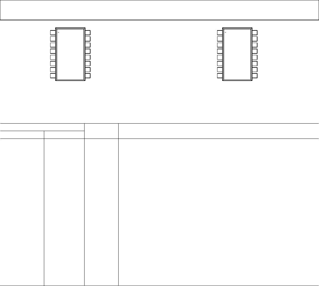
Figure 9. ADuM242D Pin Configuration
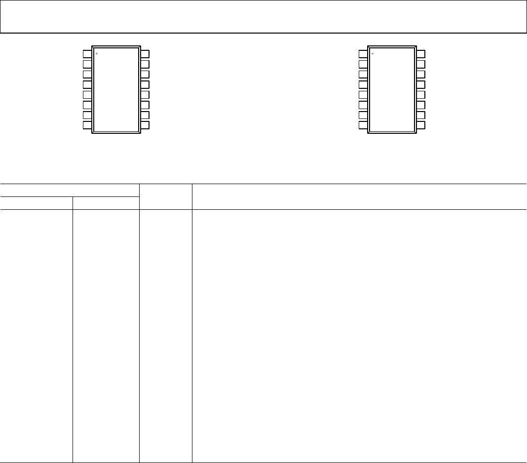
Figure 10. ADuM242E Pin Configuration
Table 23. Pin Function Descriptions
Pin No.
1
ADuM242D ADuM242E Mnemonic Description
1 1 V
DD1
Supply Voltage for Isolator Side 1.
2, 8 2, 8 GND
1
Ground Reference for Isolator Side 1.
3 3 V
IA
Logic Input A.
4 4 V
IB
Logic Input B.
5 5 V
OC
Logic Output C.
6 6 V
OD
Logic Output D.
7 Not applicable DISABLE
1
Input Disable 1. This pin disables the isolator inputs. Outputs take on the logic state
determined by the fail-safe option shown in the Ordering Guide.
Not applicable 7 V
E1
Output Enable 1. Active high logic input. When V
E1
is high or disconnected, the V
OC
and V
OD
outputs are enabled. When V
E1
is low, the V
OC
and V
OD
outputs are disabled to the high-Z
state.
9, 15 9, 15 GND
2
Ground Reference for Isolator Side 2.
10 Not applicable DISABLE
2
Input Disable 2. This pin disables the isolator inputs. Outputs take on the logic state
determined by the fail-safe option shown in the Ordering Guide.
Not applicable 10 V
E2
Output Enable 2. Active high logic input. When V
E2
is high or disconnected, the V
OA
and
V
OB
outputs are enabled. When V
E2
is low, the V
OA
and V
OB
outputs are disabled to the
high-Z state.
11 11 V
ID
Logic Input D.
12 12 V
IC
Logic Input C.
13 13 V
OB
Logic Output B.
14 14 V
OA
Logic Output A.
16 16 V
DD2
Supply Voltage for Isolator Side 2.
1
Reference the AN-1109 Application Note for specific layout guidelines.
1
2
3
4
16
15
14
13
5 12
6 11
7 10
8 9
ADuM242D
TOP VIEW
(Not to Scale)
V
DD1
GND
1
V
IA
V
IB
V
OC
V
OD
DISABLE
1
GND
1
V
DD2
GND
2
V
OA
V
OB
V
IC
V
ID
DISABLE
2
GND
2
13576-106
1
2
3
4
16
15
14
13
5 12
6 11
7 10
8 9
ADuM242E
TOP VIEW
(Not to Scale)
V
DD1
GND
1
V
IA
V
IB
V
OC
V
OD
V
E1
GND
1
V
DD2
GND
2
V
OA
V
OB
V
IC
V
ID
V
E2
GND
2
13576-107