3.0 kV rms,
Dual-Channel Digital Isolators
Data Sheet
ADuM120N/ADuM121N
Rev. B Document Feedback
Information furnished by Analog Devices is believed to be accurate and reliable. However, no
responsibility is assumed by Analog Devices for its use, nor for any infringements of patents or other
rights of third parties that may result from its use. Specifications subject to change without notice. No
license is granted by implication or otherwise under any patent or patent rights of Analog Devices.
Trademarks and registered trademarks are the property of their respective owners.
One Technology Way, P.O. Box 9106, Norwood, MA 02062-9106, U.S.A.
Tel: 781.329.4700 ©2016 Analog Devices, Inc. All rights reserved.
Technical Support www.analog.com
FEATURES
High common-mode transient immunity: 100 kV/µs typical
High robustness to radiated and conducted noise
Low propagation delay
13 ns maximum for 5 V operation
15 ns maximum for 1.8 V operation
150 Mbps minimum data rate
Safety and regulatory approvals (pending)
UL recognition: 3000 V rms for 1 minute per UL 1577
CSA Component Acceptance Notice 5A
VDE certificate of conformity
DIN V VDE V 0884-10 (VDE V 0884-10):2006-12
V
IORM
= 565 V peak
CQC certification per GB4943.1-2011
Backward compatibility
ADuM120N0 pin-compatible with ADuM1285
ADuM120N1 pin-compatible with ADuM1280 and
ADuM1200
ADuM121N0 pin-compatible with ADuM1286
ADuM121N1 pin-compatible with ADuM1281 and
ADuM1201
Low dynamic power consumption
1.8 V to 5 V level translation
High temperature operation: 125°C
Failsafe high or low options
8-lead, RoHS-compliant, SOIC package
Qualified for automotive applications
APPLICATIONS
General-purpose multichannel isolation
Industrial field bus isolation
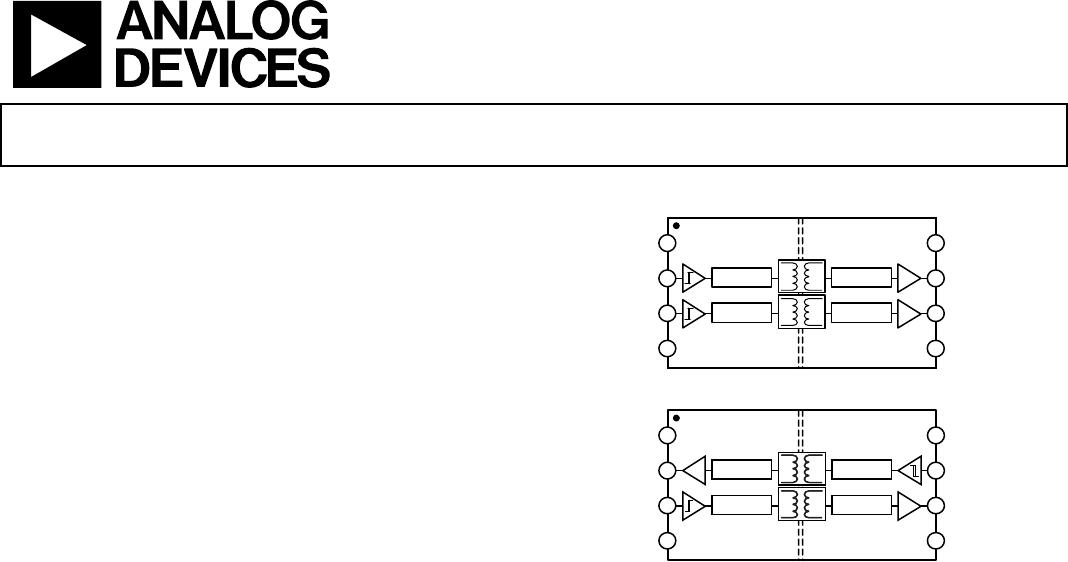
FUNCTIONAL BLOCK DIAGRAMS
ENCODE
DECODE
ENCODE DECODE
V
DD1
V
IA
V
IB
GND
1
V
DD2
V
OA
V
OB
GND
2
1
2
3
4
8
7
6
5
ADuM120N
14122-001
Figure 1. ADuM120N Functional Block Diagram
ENCODE DECODE
DECODE ENCODE
V
DD1
V
OA
V
IB
GND
1
V
DD2
V
IA
V
OB
GND
2
1
2
3
4
8
7
6
5
ADuM121N
14122-002
Figure 2. ADuM121N Functional Block Diagram
GENERAL DESCRIPTION
The ADuM120N/ADuM121N
1
are dual-channel digital isolators
based on Analog Devices, Inc., iCoupler® technology. Combining
high speed, complementary metal-oxide semiconductor (CMOS)
and monolithic air core transformer technology, these isolation
components provide outstanding performance characteristics
superior to alternatives such as optocoupler devices and other
integrated couplers. The maximum propagation delay is 13 ns
with a pulse width distortion of less than 3 ns at 5 V operation.
Channel matching is tight at 3.0 ns maximum.
The ADuM120N/ADuM121N data channels are independent and
are available in a variety of configurations with a withstand voltage
rating of 3 kV rms (see the Ordering Guide). The devices operate
with the supply voltage on either side ranging from 1.8 V to 5 V,
providing compatibility with lower voltage systems as well as
enabling voltage translation functionality across the isolation
barrier.
Unlike other optocoupler alternatives, dc correctness is ensured in
the absence of input logic transitions. Two different fail-safe options
are available in which the outputs transition to a predetermined
state when the input power supply is not applied or the inputs
are disabled.
The ADuM120N0 is pin-compatible with the ADuM1285, and
the ADuM120N1 is pin-compatible with the ADuM1280 and
the ADuM1200. The ADuM121N0 is pin-compatible with
ADuM1286, and the ADuM121N1 is pin-compatible with the
ADuM1281 and the ADuM1201.
1
Protected by U.S. Patents 5,952,849; 6,873,065; 6,903,578; and 7,075,329. Other patents are pending.
ADuM120N/ADuM121N Data Sheet
Rev. B | Page 2 of 19
TABLE OF CONTENTS
Features .............................................................................................. 1
Applications ....................................................................................... 1
Functional Block Diagrams ............................................................. 1
General Description ......................................................................... 1
Revision History ............................................................................... 2
Specifications ..................................................................................... 3
Electrical Characteristics5 V Operation................................ 3
Electrical Characteristics3.3 V Operation ............................ 5
Electrical Characteristics2.5 V Operation ............................ 7
Electrical Characteristics1.8 V Operation ............................ 9
Insulation and Safety Related Specifications .......................... 10
Package Characteristics ............................................................. 10
Regulatory Information ............................................................. 11
DIN V VDE V 0884-10 (VDE V 0884-10) Insulation
Characteristics ............................................................................ 12
Recommended Operating Conditions .................................... 12
Absolute Maximum Ratings ......................................................... 13
ESD Caution................................................................................ 13
Pin Configurations and Function Descriptions ......................... 14
Typical Performance Characteristics ........................................... 15
Applications Information .............................................................. 16
Overview ..................................................................................... 16
PCB Layout ................................................................................. 16
Propagation Delay Related Parameters ................................... 17
Jitter Measurement ..................................................................... 17
Insulation Lifetime ..................................................................... 17
Outline Dimensions ....................................................................... 19
Ordering Guide .......................................................................... 19
REVISION HISTORY
9/2016Rev. A to Rev. B
Change to General Description Section ........................................ 1
Changes to Table 11 ........................................................................ 11
4/2016Rev. 0 to Rev. A
Changes to Features Section............................................................ 1
Changes to Jitter Measurement Section ....................................... 17
Changes to Ordering Guide .......................................................... 19
Added Automotive Products Section........................................... 19
1/2016—Revision 0: Initial Version
Data Sheet ADuM120N/ADuM121N
Rev. B | Page 3 of 19
SPECIFICATIONS
ELECTRICAL CHARACTERISTICS5 V OPERATION
All typical specifications are at T
A
= 25°C, V
DD1
= V
DD2
= 5 V. M inimum/maximum specifications apply over the entire recommended
operation range of 4.5 V ≤ V
DD1
≤ 5.5 V, 4.5 V ≤ V
DD2
5.5 V, and −40°C T
A
≤ +125°C, unless otherwise noted. Switching specifications
are tested with C
L
= 15 pF and CMOS signal levels, unless otherwise noted. Supply currents are specified with 50% duty cycle signals.
Table 1.
Parameter
Symbol
Typ
Max
Unit
Test Conditions/Comments
SWITCHING SPECIFICATIONS
Pulse Width PW 6.6 ns Within pulse width distortion (PWD) limit
Data Rate 150 Mbps Within PWD limit
Propagation Delay t
PHL
, t
PLH
4.8 7.2 13 ns 50% input to 50% output
Pulse Width Distortion PWD 0.5 3 ns |t
PLH
− t
PHL
|
Change vs. Temperature 1.5 ps/°C
Propagation Delay Skew t
PSK
6.0 ns Between any two units at the same
temperature, voltage, and load
Channel Matching
Codirectional t
PSKCD
0.5 3.0 ns
Opposing Direction t
PSKOD
0.5 3.0 ns
Jitter 380 ps p-p See the Jitter Measurement section
55
ps rms
See the Jitter Measurement section
DC SPECIFICATIONS
Input Threshold Voltage
Logic High V
IH
0.7 × V
DDx
V
Logic Low V
IL
0.3 × V
DDx
V
Output Voltage
Logic High V
OH
V
DDx
− 0.1 V
DDx
V I
Ox
1
= −20 µA, V
Ix
= V
IxH
2
V
DDx
− 0.4 V
DDx
− 0.2 V I
Ox
1
= −4 mA, V
Ix
= V
IxH
2
Logic Low V
OL
0.0 0.1 V I
Ox
1
= 20 µA, V
Ix
= V
IxL
3
0.2
0.4
V
I
Ox
1
= 4 mA, V
Ix
= V
IxL
3
Input Current per Channel I
I
−10 +0.01 +10 µA 0 V ≤ V
Ix
V
DDx
Quiescent Supply Current
ADuM120N I
DD1 (Q)
0.9 1.3 mA V
I
4
= 0 (N0), 1 (N1)
5
I
DD2 (Q)
1.3 1.8 mA V
I
4
= 0 (N0), 1 (N1)
5
I
DD1 (Q)
6.4
10.0
mA
V
I
4
= 1 (N0), 0 (N1)
5
I
DD2 (Q)
1.4 1.9 mA V
I
4
= 1 (N0), 0 (N1)
5
ADuM121N I
DD1 (Q)
1.1 1.6 mA V
I
4
= 0 (N0), 1 (N1)
5
I
DD2 (Q)
1.1 1.5 mA V
I
4
= 0 (N0), 1 (N1)
5
I
DD1 (Q)
4.0 5.8 mA V
I
4
= 1 (N0), 0 (N1)
5
I
DD2 (Q)
4.9 6.4 mA V
I
4
= 1 (N0), 0 (N1)
5
Dynamic Supply Current
Dynamic Input I
DDI (D)
0.01 mA/Mbps Inputs switching, 50% duty cycle
Dynamic Output I
DDO (D)
0.02 mA/Mbps Inputs switching, 50% duty cycle
Undervoltage Lockout UVLO
Positive V
DDx
Threshold V
DDxUV+
1.6 V
Negative V
DDx
Threshold V
DDxUV−
1.5 V
V
DDx
Hysteresis V
DDxUVH
0.1 V

ADUM120N1BRZ-RL7

Mfr. #:
Manufacturer:
Analog Devices Inc.
Description:
Digital Isolators 2ch EMC robust 3kV digital Isolator 2/0
Lifecycle:
New from this manufacturer.
Delivery:
DHL FedEx Ups TNT EMS
Payment:
T/T Paypal Visa MoneyGram Western Union