Data Sheet ADuM120N/ADuM121N
Rev. B | Page 13 of 19
ABSOLUTE MAXIMUM RATINGS
T
A
= 25°C, unless otherwise noted.
Table 14.
Parameter Rating
Supply Voltages (V
DD1
, V
DD2
) −0.5 V to +7.0 V
Input Voltages (V
IA
, V
IB
)
1
−0.5 V to V
DDI
+ 0.5 V
Output Voltages (V
OA
, V
OB
)
2
−0.5 V to V
DDO
+ 0.5 V
Average Output Current per Pin
3
Side 1 Output Current (I
O1
) −10 mA to +10 mA
Side 2 Output Current (I
O2
) −10 mA to +10 mA
Common-Mode Transients
4
−150 kV/µs to +150 kV/µs
Storage Temperature (T
ST
) Range −65°C to +150°C
Ambient Operating Temperature
(T
A
) Range
−40°C to +125°C
1
V
DDI
is the input side supply voltage.
2
V
DDO
is the output side supply voltage.
3
See Figure 3 for the maximum rated current values for various temperatures.
4
Common-mode transients refer to the common-mode transients across the
insulation barrier. Common-mode transients exceeding the absolute
maximum ratings can cause latch-up or permanent damage.
Stresses at or above those listed under Absolute Maximum
Ratings may cause permanent damage to the product. This is a
stress rating only; functional operation of the product at these
or any other conditions above those indicated in the operational
section of this specification is not implied. Operation beyond
the maximum operating conditions for extended periods may
affect product reliability.
ESD CAUTION
Table 15. Maximum Continuous Working Voltage
1
Parameter
Rating
Constraint
2
AC VOLTAGE Lifetime limited by package creepage maximum approved working voltage per IEC 60950-1
Bipolar Waveform
Basic Insulation 789 V peak
Reinforced Insulation 403 V peak
Unipolar Waveform
Basic Insulation 909 V peak
Reinforced Insulation 469 V peak
DC V OLTAGE Lifetime limited by package creepage maximum approved working voltage per IEC 60950-1
Basic Insulation 558 V peak
Reinforced Insulation
285 V peak
1
Maximum continuous working voltage refers to the continuous voltage magnitude imposed across the isolation barrier. See the Insulation Lifetime section for more details.
2
Insulation lifetime for the specified test condition is greater than 50 years.
Truth Tables
Table 16. ADuM120N/ADuM121N Truth Table (Positive Logic)
V
Ix
Input
1
V
DDI
State
1
V
DDO
State
1
Default Low (N0),
V
Ox
Output
1, 2
Default High (N1),
V
Ox
Output
1, 2
Test Conditions/Comments
Low Powered Powered Low Low Normal operation
High Powered Powered High High Normal operation
Don’t Care
3
Unpowered Powered Low High Fail-safe output
Don’t Care
3
Powered Unpowered Indeterminate Indeterminate
1
V
Ix
and V
Ox
refer to the input and output signals of a given channel (A or B). V
DDI
and V
DDO
refer to the supply voltages on the input and output sides of the given
channel, respectively.
2
N0 is the ADuM120N0/ADuM121N0 models, N1 is the ADuM120N1/ADuM121N1 models. See the Ordering Guide.
3
Input pins (V
Ix
) on the same side as an unpowered supply must be in a low state to avoid powering the device through the ESD protection circuitry.
ADuM120N/ADuM121N Data Sheet
Rev. B | Page 14 of 19
PIN CONFIGURATIONS AND FUNCTION DESCRIPTIONS
1
8
2
7
3
6
4
5
TOP VIEW
(Not to Scale)
ADuM120N
V
DD1
V
IA
V
IB
GND
1
V
DD2
V
OA
V
OB
GND
2
14122-004
Figure 4. ADuM120N Pin Configuration
Reference the AN-1109 Application Note for specific layout guidelines.
Table 17. ADuM120N Pin Function Descriptions
Pin No. Mnemonic Description
1 V
DD1
Supply Voltage for Isolator Side 1.
2 V
IA
Logic Input A.
3 V
IB
Logic Input B.
4 GND
1
Ground 1. This pin is the ground reference for Isolator Side 1.
5 GND
2
Ground 2. This pin is the ground reference for Isolator Side 2.
6 V
OB
Logic Output B.
7 V
OA
Logic Output A.
8 V
DD2
Supply Voltage for Isolator Side 2.
1
8
2 7
3 6
4 5
TOP VIEW
(Not to Scale)
ADuM121N
V
DD1
V
OA
V
IB
GND
1
V
DD2
V
IA
V
OB
GND
2
14122-005
Figure 5. ADuM121N Pin Configuration
Reference the AN-1109 Application Note for specific layout guidelines.
Table 18. ADuM121N Pin Function Descriptions
Pin No. Mnemonic Description
1 V
DD1
Supply Voltage for Isolator Side 1.
2 V
OA
Logic Output A.
3 V
IB
Logic Input B.
4 GND
1
Ground 1. This pin is the ground reference for Isolator Side 1.
5 GND
2
Ground 2. This pin is the ground reference for Isolator Side 2.
6
V
OB
Logic Output B.
7 V
IA
Logic Input A.
8 V
DD2
Supply Voltage for Isolator Side 2.
Data Sheet ADuM120N/ADuM121N
Rev. B | Page 15 of 19
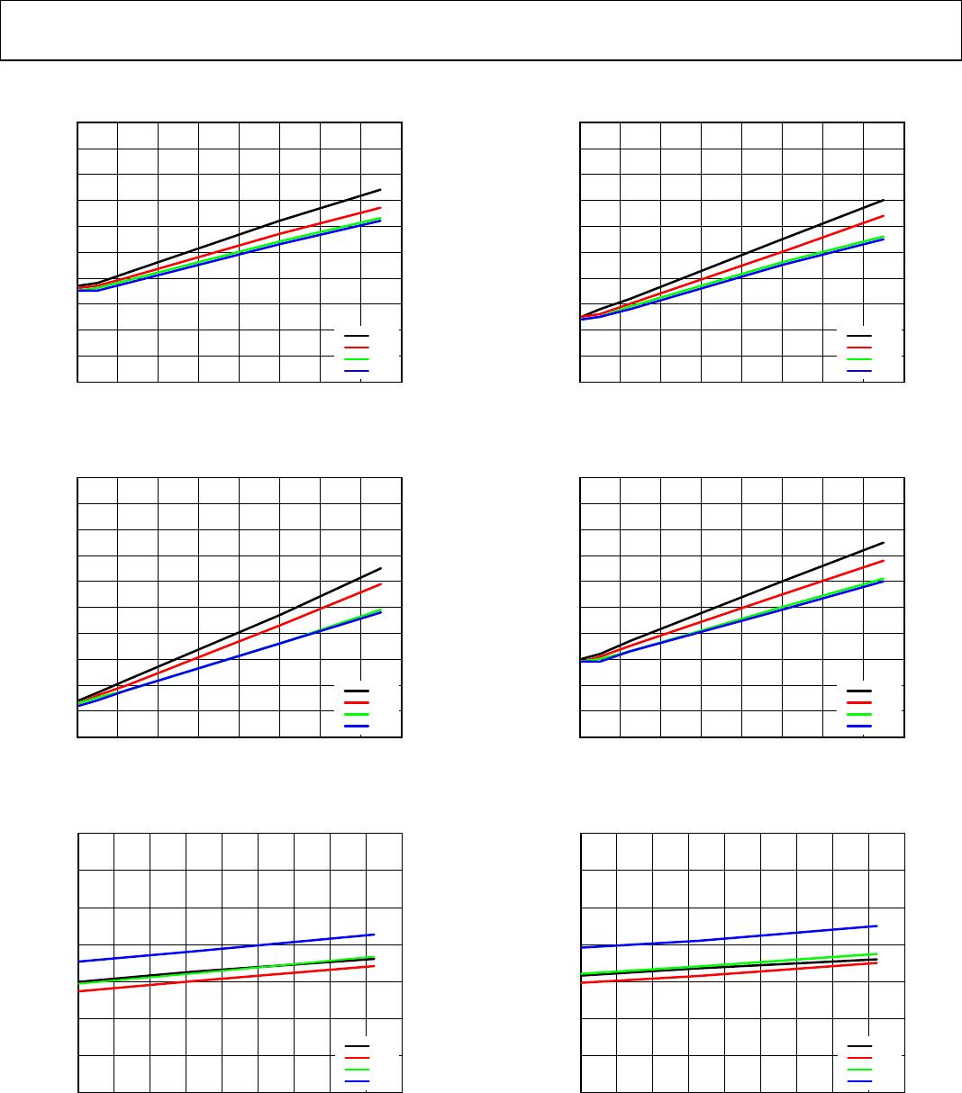
TYPICAL PERFORMANCE CHARACTERISTICS
10
0
1
2
3
4
5
6
7
8
9
0 20 40 60 80 100 120 140 160
I
DD1
SUPPLY CURRENT (mA)
DATA RATE (Mbps)
14122-106
5V
3.3V
2.5V
1.8V
Figure 6. ADuM120N I
DD1
Supply Current vs. Data Rate at Various Voltages
10
0
1
2
3
4
5
6
7
8
9
0 20 40 60 80 100 120 140 160
I
DD2
SUPPLY CURRENT (mA)
DATA RATE (Mbps)
14122-109
5V
3.3V
2.5V
1.8V
Figure 7. ADuM120N I
DD2
Supply Current vs. Data Rate at Various Voltages
14
0
2
4
6
8
10
12
–40 –20 0 20 40 60 80 100 120 140
PROPAGATION DELAY,
t
PLH
(ns)
TEMPERATURE (°C)
14122-108
5V
3.3V
2.5V
1.8V
Figure 8. Propagation Delay for Logic High Output (t
PLH
) vs. Temperature at
Various Voltages
10
0
1
2
3
4
5
6
7
8
9
0 20 40 60 80 100 120 140 160
I
DD1
SUPPLY CURRENT (mA)
DATA RATE (Mbps)
14122-107
5V
3.3V
2.5V
1.8V
Figure 9. ADuM121N I
DD1
Supply Current vs. Data Rate at Various Voltages
10
0
1
2
3
4
5
6
7
8
9
0 20 40 60 80 100 120 140 160
I
DD2
SUPPLY CURRENT (mA)
DATA RATE (Mbps)
14122-110
5V
3.3V
2.5V
1.8V
Figure 10. ADuM121N I
DD2
Supply Current vs. Data Rate at Various Voltages
14
0
2
4
6
8
10
12
–40 –20 0 20 40 60 80 100 120 140
PROPAGATION DELAY,
t
PHL
(ns)
TEMPERATURE (°C)
14122-111
5V
3.3V
2.5V
1.8V
Figure 11. Propagation Delay for Logic Low Output (t
PHL
) vs. Temperature at
Various Voltages

ADUM120N1BRZ-RL7

Mfr. #:
Manufacturer:
Analog Devices Inc.
Description:
Digital Isolators 2ch EMC robust 3kV digital Isolator 2/0
Lifecycle:
New from this manufacturer.
Delivery:
DHL FedEx Ups TNT EMS
Payment:
T/T Paypal Visa MoneyGram Western Union