Data Sheet ADuM120N/ADuM121N
Rev. B | Page 17 of 19
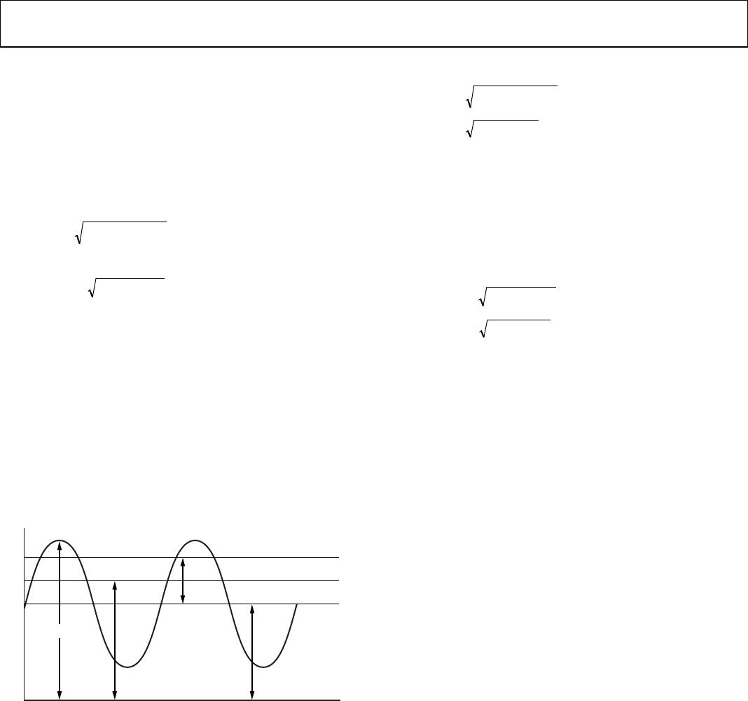
PROPAGATION DELAY RELATED PARAMETERS
Propagation delay is a parameter that describes the time it takes
a logic signal to propagate through a component. The propagation
delay to a Logic 0 output can differ from the propagation delay
to a Logic 1 output.
INPUT (V
Ix
)
OUTPUT (V
Ox
)
t
PLH
t
PHL
50%
50%
14122-013
Figure 15. Propagation Delay Parameters
Pulse width distortion is the maximum difference between these
two propagation delay values and is an indication of how
accurately the timing of the input signal is preserved.
Channel matching is the maximum amount the propagation delay
differs between channels within a single ADuM120N/ADuM121N
component.
Propagation delay skew is the maximum amount the propagation
delay differs between multiple ADuM120N/ADuM121N
components operating under the same conditions
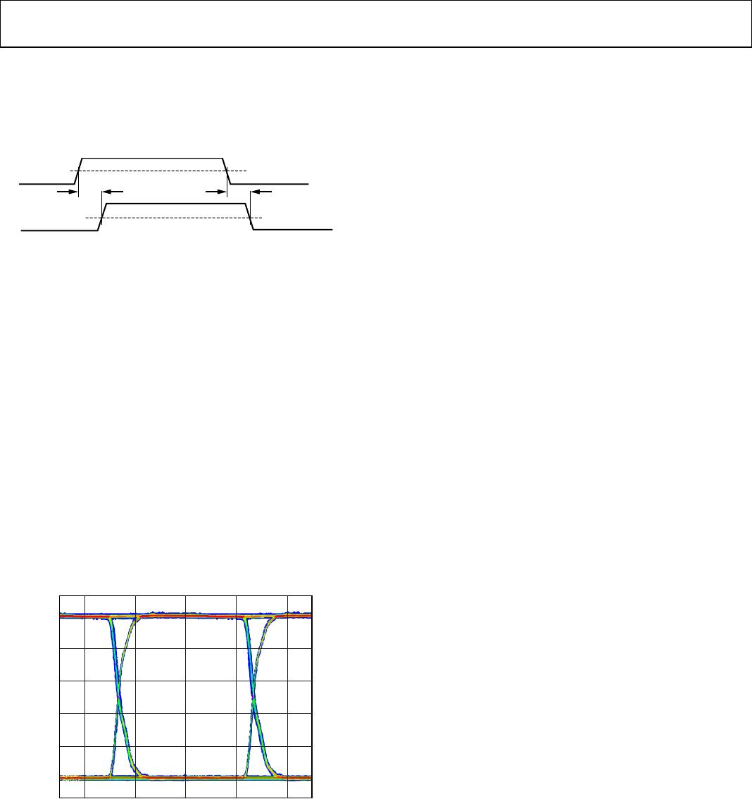
JITTER MEASUREMENT
Figure 16 shows the eye diagram for the ADuM120N/ADuM121N.
The measurement was taken using an Agilent 81110A pulse
pattern generator at 150 Mbps with pseudorandom bit sequences
(PRBS) 2(n − 1), n = 14, for 5 V supplies. Jitter was measured
with the Tektronix Model 5104B oscilloscope, 1 GHz, 10 GS/s
with the DPOJET jitter and eye diagram analysis tools. The result
shows a typical measurement on the ADuM120N/ADuM121N
with 380 ps p-p jitter.
105
0
1
2
3
4
VOLTAGE (V)
5
0
TIME (ns)
–5–10
14122-014
Figure 16. ADuM120N/ADuM121N Eye Diagram
INSULATION LIFETIME
All insulation structures eventually break down when subjected
to voltage stress over a sufficiently long period. The rate of
insulation degradation is dependent on the characteristics of the
voltage waveform applied across the insulation as well as on the
materials and material interfaces.
The two types of insulation degradation of primary interest are
breakdown along surfaces exposed to the air and insulation wear
out. Surface breakdown is the phenomenon of surface tracking
and the primary determinant of surface creepage requirements
in system level standards. Insulation wear out is the phenomenon
where charge injection or displacement currents inside the
insulation material cause long-term insulation degradation.
Surface Tracking
Surface tracking is addressed in electrical safety standards by
setting a minimum surface creepage based on the working voltage,
the environmental conditions, and the properties of the insulation
material. Safety agencies perform characterization testing on the
surface insulation of components that allows the components to be
categorized in different material groups. Lower material group
ratings are more resistant to surface tracking and, therefore, can
provide adequate lifetime with smaller creepage. The minimum
creepage for a given working voltage and material group is in each
system level standard and is based on the total rms voltage
across the isolation, pollution degree, and material group. The
material group and creepage for the ADuM120N/ADuM121N
isolators are presented in Table 9.
Insulation Wear Out
The lifetime of insulation caused by wear out is determined by
the thickness, material properties, and the voltage stress applied.
It is important to verify that the product lifetime is adequate at
the application working voltage. The working voltage supported
by an isolator for wear out cannot be the same as the working
voltage supported for tracking. It is the working voltage applicable
to tracking that is specified in most standards.
Testing and modeling show that the primary driver of long-term
degradation is displacement current in the polyimide insulation
causing incremental damage. The stress on the insulation can be
broken down into broad categories, such as dc stress, which
causes very little wear out because there is no displacement
current, and an ac component time varying voltage stress,
which causes wear out.