VS-VSKT26.., VS-VSKH26.., VS-VSKL26.., VS-VSKN26.. Series
www.vishay.com
Vishay Semiconductors
Revision: 21-Mar-14
3
Document Number: 94629
For technical questions within your region: DiodesAmericas@vishay.com
, DiodesAsia@vishay.com, DiodesEurope@vishay.com
THIS DOCUMENT IS SUBJECT TO CHANGE WITHOUT NOTICE. THE PRODUCTS DESCRIBED HEREIN AND THIS DOCUMENT
ARE SUBJECT TO SPECIFIC DISCLAIMERS, SET FORTH AT www.vishay.com/doc?91000
Note
• Table shows the increment of thermal resistance R
thJC
when devices operate at different conduction angles than DC
TRIGGERING
PARAMETER SYMBOL TEST CONDITIONS VALUES UNITS
Maximum peak gate power P
GM
10
W
Maximum average gate power P
G(AV)
2.5
Maximum peak gate current I
GM
2.5 A
Maximum peak negative gate voltage - V
GM
10
V
Maximum gate voltage required to trigger V
GT
T
J
= -40 °C
Anode supply = 6 V
resistive load
4.0
T
J
= 25 °C 2.5
T
J
= 125 °C 1.7
Maximum gate current required to trigger I
GT
T
J
= -40 °C
Anode supply = 6 V
resistive load
270
mAT
J
= 25 °C 150
T
J
= 125 °C 80
Maximum gate voltage that will not trigger V
GD
T
J
= 125 °C, rated V
DRM
applied 0.25 V
Maximum gate current that will not trigger I
GD
T
J
= 125 °C, rated V
DRM
applied 6 mA
BLOCKING
PARAMETER SYMBOL TEST CONDITIONS VALUES UNITS
Maximum peak reverse and off-state
leakage current at V
RRM
, V
DRM
I
RRM,
I
DRM
T
J
= 125 °C, gate open circuit 15 mA
Maximum RMS insulation voltage V
INS
50 Hz
3000 (1 min)
3600 (1 s)
V
Maximum critical rate of rise of off-state voltage dV/dt T
J
= 125 °C, linear to 0.67 V
DRM
1000 V/μs
THERMAL AND MECHANICAL SPECIFICATIONS
PARAMETER SYMBOL TEST CONDITIONS VALUES UNITS
Junction operating and storage
temperature range
T
J
, T
Stg
-40 to 125 °C
Maximum internal thermal resistance,
junction to case per leg
R
thJC
DC operation 0.76
°C/W
Typical thermal resistance,
case to heatsink per module
R
thCS
Mounting surface flat, smooth and greased 0.1
Mounting torque ± 10 %
to heatsink
A mounting compound is recommended and the
torque should be rechecked after a period of
3 hours to allow for the spread of the compound.
4
Nm
busbar 3
Approximate weight
75 g
2.7 oz.
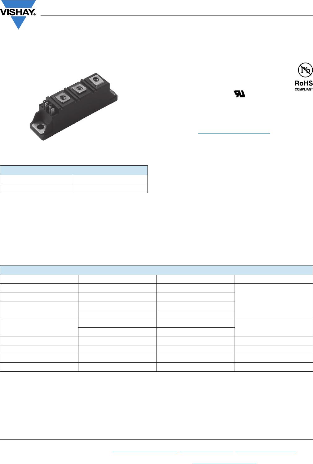
Case style JEDEC
®
AAP GEN VII (TO-240AA)
R CONDUCTION PER JUNCTION
DEVICES
SINE HALF WAVE CONDUCTION RECTANGULAR WAVE CONDUCTION
UNITS
180° 120° 90° 60° 30° 180° 120° 90° 60° 30°
VSK.26.. 0.212 0.258 0.330 0.466 0.72 0.166 0.276 0.357 0.482 0.726 °C/W