AMIS30522, NCV70522
http://onsemi.com
19
Charge Pump Failure
The charge pump is an important circuit that guarantees
low R
DS(on)
for all drivers, especially for low supply
voltages. If the supply voltage is too low or external
components are not properly connected to guarantee R
DS(on)
of the drivers, then the bit <CPFAIL> is set in the SPI Status
Register 0. Also after poweronreset the charge pump
voltage will need some time to exceed the required
threshold. During that time <CPFAIL> will be set to “1”.
Error Output
This is an open drain digital output to flag a problem to the
external microcontroller. The signal on this output is active
low and the logic combination of:
NOT(ERR
) = <TW> OR <TSD> OR <OVCXij> OR
<OVCYij> OR <OPENi> OR <CPFAIL>
Logic Supply Regulator
The 522 has an onchip 5 V lowdrop regulator with
external capacitor to supply the digital part of the chip, some
lowvoltage analog blocks and external circuitry. The
voltage level is derived from an internal bandgap reference.
To calculate the available drivecurrent for external
circuitry, the specified I
load
should be reduced with the
consumption of internal circuitry (unloaded outputs) and the
loads connected to logic outputs. See Table 5.
PowerOn Reset (POR) Function
The open drain output pin POR/WD provides an “active
low” reset for external purposes. At powerup of
AMIS30522/NCV70522, this pin will be kept low for
some time to reset for example an external microcontroller.
A small analog filter avoids resetting due to spikes or noise
on the V
DD
supply.
Figure 15. PoweronReset Timing Diagram
VBB
VDD
t
t
V
DDH
V
DDL
POR/WD pin
t
PU
t
PD
< t
RF
t
POR
t
RF
Watchdog Function
The watchdog function is enabled/disabled through
<WDEN> bit (Table 13). Once this bit has been set to “1”
(watchdog enable), the microcontroller needs to rewrite
this bit to clear an internal timer before the watchdog timeout
interval expires. In case the timer is activated and WDEN is
acknowledged too early (before t
WDPR
) or not within the
interval (after t
WDTO
), then a reset of the microcontroller
will occur through POR
/WD pin. In addition, a warm/cold
boot bit <WD> is available in Table 16 for further processing
when the external microcontroller is alive again.
AMIS30522, NCV70522
http://onsemi.com
20
VBB
VDD
t
t
Enable WD
Acknowledge WD
WD timer
t
t
Figure 16. Watchdog Timing Diagram
V
DDH
t
PU
t
POR
t
DSPI
POR/WD pin
t
WDTO
t
POR
t
WDRD
= t
WDPR
or = t
WDTO
> t
WDPR
and < t
WDTO
Note: t
DSPI
is the time needed by the external
microcontroller to shiftin the <WDEN> bit after a
powerup.
The duration of the watchdog timeout interval is
programmable through the WDT[3:0] bits. The timing is
given in Figure 16.
CLR Pin (=Hard Reset)
Logic 0 on CLR pin allows normal operation of the chip.
To reset the complete digital inside the 522, the input CLR
needs to be pulled to logic 1 during minimum time given by
t
CLR
. (See AC Parameters) This reset function clears all
internal registers without the need of a powercycle, except
in sleep mode. The operation of all analog circuits is
depending on the reset state of the digital, charge pump
remains active. Logic 0 on CLR pin resumes normal
operation again. The voltage regulator remains functional
during and after the reset and the POR
/WD pin is not
activated. Watchdog function is reset completely.
Sleep Mode
The bit <SLP> in SPI Control Register 2 is provided to
enter a socalled “sleep mode”. This mode allows reduction
of currentconsumption when the motor is not in operation.
The effect of sleep mode is as follows:
The drivers are put in HiZ
All analog circuits are disabled and in lowpower mode
All internal registers are maintaining their logic content
NXT and DIR inputs are ignored
SPI communication remains possible (slight current
increase during SPI communication)
Oscillator and digital clocks are silent, except during
SPI communication
Normal operation is resumed after writing logic ‘0’ to bit
<SLP>. A startup time is needed for the charge pump to
stabilize. After this time, NXT commands can be issued.
When the device is in sleep mode and V
BB
becomes lower
than V
BB_min
the device might reset.
AMIS30522, NCV70522
http://onsemi.com
21
SPI INTERFACE
The serial peripheral interface (SPI) allows an external
microcontroller (Master) to communicate with the 522. The
implemented SPI block is designed to interface directly with
numerous microcontrollers from several manufacturers.
The 522 acts always as a Slave and cannot initiate any
transmission. The operation of the device is configured and
controlled by means of SPI registers which are observable
for read and/or write from the Master.
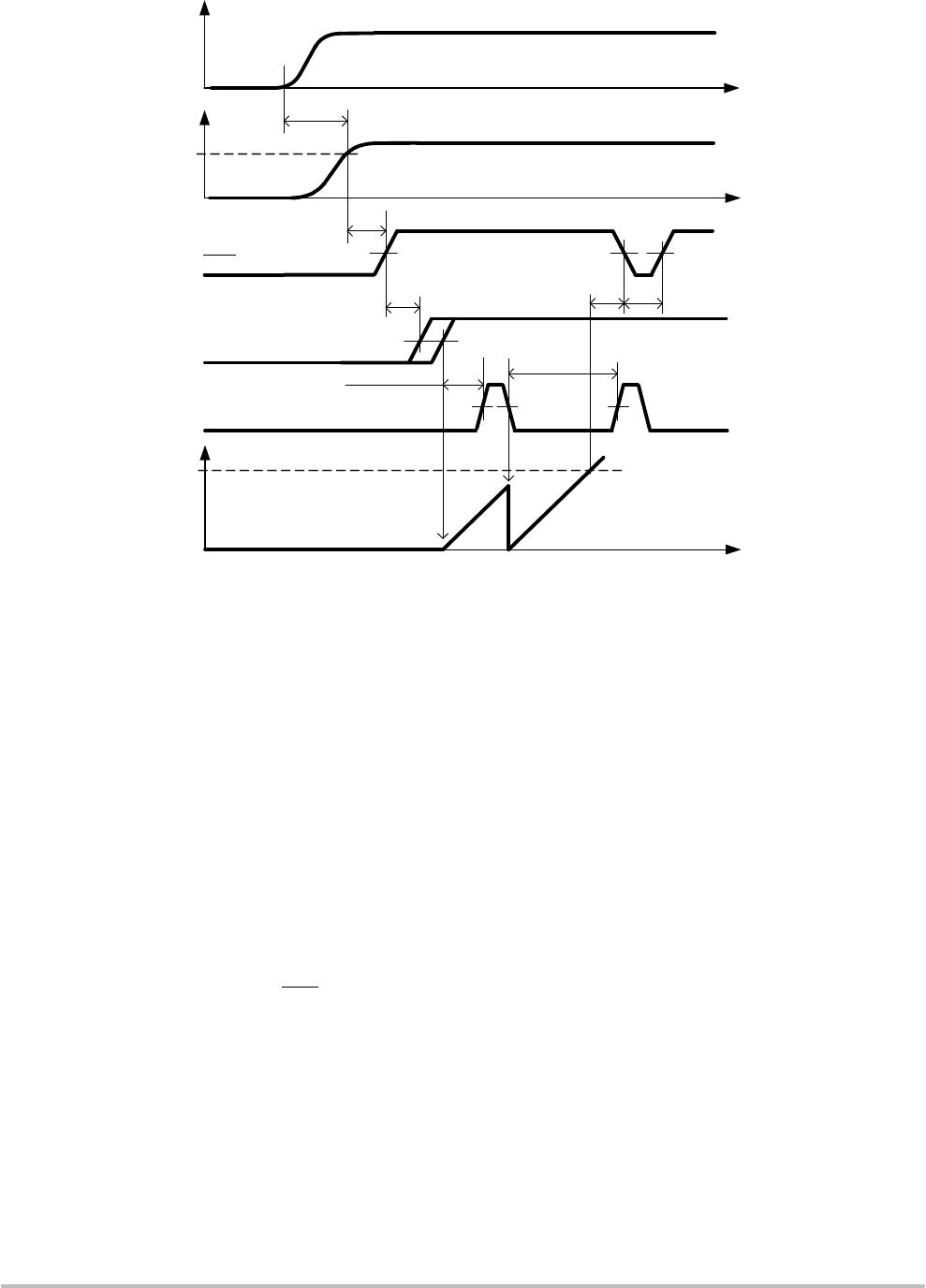
SPI Transfer Format and Pin Signals
During a SPI transfer, data is simultaneously transmitted
(shifted out serially) and received (shifted in serially). A
serial clock line (CLK) synchronizes shifting and sampling
of the information on the two serial data lines (DO and DI).
DO signal is the output from the Slave (522), and DI signal
is the output from the Master. A chip select line (CS
) allows
individual selection of a Slave SPI device in a multiple
slave system. The CS
line is active low. If the 522 is not
selected, DO is pulled up with the external pullup resistor.
Since 522 operates as a Slave in MODE 0 (CPOL = 0; CPHA
= 0) it always clocks data out on the falling edge and samples
data in on rising edge of clock. The Master SPI port must be
configured in MODE 0 too, to match this operation. The SPI
clock idles low between the transferred bytes.
The diagram below is both a Master and a Slave timing
diagram since CLK, DO and DI pins are directly connected
between the Master and the Slave.
DI
MSB
CLK
1 2 3 4 5 6 7 8
DO
#CLK Cycle
MSB
LSB
LSB
654321
654321
Figure 17. Timing Diagram of a SPI Transfer
CS
NOTE: At the falling edge of the eighth clock pulse the dataout shift register is updated with the content of the addressed internal SPI
register. The internal SPI registers are updated at the first rising edge of the 522 system clock when CS
= High.
Transfer Packet
Serial data transfer is assumed to follow MSB first rule. The transfer packet contains one or more bytes.
LSB
DataCommand and SPI Register Address
CMD2 CMD1 CMD0 ADDR4 ADDR3 ADDR2 ADDR1 ADDR0
D7 D6 D5 D4 D3 D2 D1 D0
MSBLSBMSB
BYTE 1
BYTE 2
Command
SPI Register Address
Figure 18. SPI Transfer Packet
Byte 1 contains the Command and the SPI Register
Address and indicates to the 522 the chosen type of
operation and addressed register. Byte 2 contains data, or
sent from the Master in a WRITE operation, or received
from the 522 in a READ operation.
Two command types can be distinguished in the
communication between Master and 522:
READ from SPI Register with address ADDR[4:0]:
CMD[2:0] = “000”
WRITE to SPI Register with address ADDR[4:0]:
CMD[2:0] = “100”

AMIS30522C5222G

Mfr. #:
Manufacturer:
ON Semiconductor
Description:
Motor / Motion / Ignition Controllers & Drivers 800MA STEPPER DRVR
Lifecycle:
New from this manufacturer.
Delivery:
DHL FedEx Ups TNT EMS
Payment:
T/T Paypal Visa MoneyGram Western Union

Products related to this Datasheet