AMIS30522, NCV70522
http://onsemi.com
25
WDT[3:0] Selects the watchdog timeout interval.
Table 13. WATCHDOG TIMEOUT INTERVAL AS FUNCTION OF WDT[3:0]
Index WDT[3:0] t
WDTO
(ms)
0 0 0 0 0 32
1 0 0 0 1 64
2 0 0 1 0 96
3 0 0 1 1 128
4 0 1 0 0 160
5 0 1 0 1 192
6 0 1 1 0 224
7 0 1 1 1 256
Index WDT[3:0] t
WDTO
(ms)
8 1 0 0 0 288
9 1 0 0 1 320
A 1 0 1 0 352
B 1 0 1 1 384
C 1 1 0 0 416
D 1 1 0 1 448
E 1 1 1 0 480
F 1 1 1 1 512
CUR[4:0] Selects IMCmax peak. This is the peak or amplitude of the regulated current waveform in the motor coils.
Table 14. SPI CONTROL PARAMETER OVERVIEW: CURRENT AMPLITUDE CUR[4:0]
Current Range
(Note 17)
Index CUR[4:0]
Current (mA)
(Note 16)
Current Range
(Note 17)
Index CUR[4:0]
Current (mA)
(Note 16)
0
0 00000 33
2
16 10000 365
1 00001 64 17 10001 400
2 00010 95 18 10010 440
3 00011 104 19 10011 485
4 00100 115 20 10100 530
5 00101 126 21 10101 585
6 00110 138 22 10110 630
7 00111 153
3
23 10111 750
8 01000 166 24 11000 825
1
9 01001 190 25 11001 895
10 01010 205 26 11010 975
11 01011 230 27 11011 1065
12 01100 250 28 11100 1155
13 01101 275 29 11101 1245
14 01110 300 30 11110 1365
15 01111 325 31 11111 1480
16.Typical current amplitude at T
J
= 125°C.
17.Reducing the current over different current ranges might trigger overcurrent detection, please refer to dedicated application note for solutions.
SPI Status Register Description
All 4 SPI Status Registers have Read Access and are default to “0” after Poweron or hard reset.
Table 15. SPI STATUS REGISTERS
Address
Content
Structure
Bit 7 Bit 6 Bit 5 Bit 4 Bit 3 Bit 2 Bit 1 Bit 0
Access R R R R R R R R
Reset 0 0 0 0 0 0 0 0
SR0 04h Data Not Latched PAR TW CPfail WD OPENX OPENY
SR1 05h Data is Latched PAR OVCXPT OVCXPB OVCXNT OVCXNB
SR2 06h Data is Latched PAR OVCYPT OVCYPB OVCYYNT OVCYNB TSD
SR3 07h Data Not Latched PAR MSP[6:0]
Where:
R: Read only mode access
Reset: Status after PowerOn or hard reset
PAR: Parity check
AMIS30522, NCV70522
http://onsemi.com
26
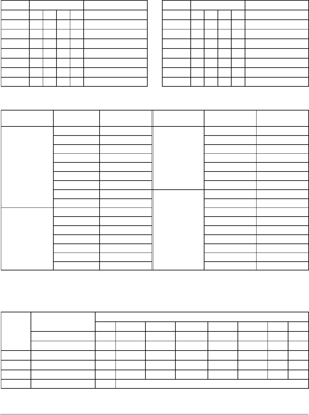
Table 16. SPI STATUS FLAGS OVERVIEW
Mnemonic Flag
Length
(bit)
Related
SPI Register
Comment
Reset
State
CPFail Charge Pump Failure 1 Status Register 0
‘0’ = no failure
‘1’ = failure: indicates that the charge pump does not
reach the required voltage level.
‘0’
WD Watchdog event 1 Status Register 0
This bit indicates the watchdog timer has not been
cleared properly in time. If the master reads that WD
is set to “1” after reset, it means that a watchdog re-
set occurred (warm boot) instead of poweronreset
(cold boot). WD bit will be cleared only when the
master writes “0” to WDEN bit.
‘0’
MSP[6:0] Micro Step Position 7 Status Register 3 Translator micro step position ‘0000000’
OPENX OPEN Coil X 1 Status Register 0 ‘1’ = Open coil detected ‘0’
OPENY OPEN Coil Y 1 Status Register 0 ‘1’ = Open coil detected ‘0’
OVCXNB
Overcurrent at
MOTXN Terminal;
Bottom Transistor
1 Status Register 1
‘0’ = no failure
‘1’ = failure: indicates that overcurrent is detected at
bottom transistor XNterminal
‘0’
OVCXNT
Overcurrent at
MOTXN Terminal;
Top Transistor
1 Status Register 1
‘0’ = no failure
‘1’ = failure: indicates that overcurrent is detected at
top transistor XNterminal
‘0’
OVCXPB
Overcurrent at
MOTXP Terminal;
Bottom Transistor
1 Status Register 1
‘0’ = no failure
‘1’ = failure: indicates that overcurrent is detected at
bottom transistor XPterminal
‘0’
OVCXPT
Overcurrent at
MOTXP Terminal;
Top Transistor
1 Status Register 1
‘0’ = no failure
‘1’ = failure: indicates that overcurrent is detected at
top transistor XPterminal
‘0’
OVCYNB
Overcurrent at
MOTYN Terminal;
Bottom Transistor
1 Status Register 2
‘0’ = no failure
‘1’ = failure: indicates that overcurrent is detected at
bottom transistor YNterminal
‘0’
OVCYNT
Overcurrent at
MOTYN Terminal;
Top Transistor
1 Status Register 2
‘0’ = no failure
‘1’ = failure: indicates that overcurrent is detected at
top transistor YNterminal
‘0’
OVCYPB
Overcurrent at
MOTYP Terminal;
Bottom Transistor
1 Status Register 2
‘0’ = no failure
‘1’ = failure: indicates that overcurrent is detected at
bottom transistor YPterminal
‘0’
OVCYPT
Overcurrent at
MOTYP Terminal;
Top Transistor
1 Status Register 2
‘0’ = no failure
‘1’ = failure: indicates that overcurrent is detected at
top transistor YPterminal
‘0’
TSD Thermal Shutdown 1 Status Register 2 ‘0’
TW Thermal Warning 1 Status Register 0 ‘0’
WD Watchdog event 1 Status Register 0
‘0’ = no watchdog reset
‘1’ = watchdog reset occurred
‘0’
AMIS30522, NCV70522
http://onsemi.com
27
DEVICE ORDERING INFORMATION
Part Number
Ambient
Temperature Range
Package Type
Peak
Current
Shipping
AMIS30522C5222RG 40°C to +125°C NQFP32
(PbFree)
1500 mA Tape & Reel
AMIS30522C5222G 40°C to +125°C NQFP32
(PbFree)
1500 mA Tube / Tray
NCV70522MN003R2G* 40°C to +125°C NQFP32
(PbFree)
1500 mA Tape & Reel
NCV70522MN003G* 40°C to +125°C NQFP32
(PbFree)
1500 mA Tube / Tray
For information on tape and reel specifications, including part orientation and tape sizes, please refer to our Tape and Reel Packaging
Specifications Brochure, BRD8011/D.
*Qualified for automotive applications.

AMIS30522C5222G

Mfr. #:
Manufacturer:
ON Semiconductor
Description:
Motor / Motion / Ignition Controllers & Drivers 800MA STEPPER DRVR
Lifecycle:
New from this manufacturer.
Delivery:
DHL FedEx Ups TNT EMS
Payment:
T/T Paypal Visa MoneyGram Western Union

Products related to this Datasheet