AMIS30522, NCV70522
http://onsemi.com
4
Table 2. ABSOLUTE MAXIMUM RATINGS
Symbol Parameter Min Max Unit
V
BB
Analog DC Supply Voltage (Note 1) 0.3 +40 V
T
ST
Storage Temperature 55 +160 °C
T
J
Junction Temperature (Note 2) 50 +175 °C
V
ESD
Electrostatic Discharges on Component Level, All Pins (Note 3) 2 +2 kV
V
ESD
Electrostatic Discharges on Component Level, HiV Pins (Note 4) 8 +8 kV
Stresses exceeding Maximum Ratings may damage the device. Maximum Ratings are stress ratings only. Functional operation above the
Recommended Operating Conditions is not implied. Extended exposure to stresses above the Recommended Operating Conditions may affect
device reliability.
1. For limited time < 0.5 s
2. Circuit functionality not guaranteed.
3. Human Body Model (100 pF via 1.5 kW, according to JEDEC EIAJESD22A114B)
4. HiV = High Voltage Pins MOTxx, V
BB
, GND; Human Body Model (100 pF via 1.5 kW, according to JEDEC EIAJESD22A114B)
Table 3. THERMAL RESISTANCE
Package
Thermal Resistance
Unit
JunctiontoExposed Pad
JunctiontoAmbient
1S0P Board 2S2P Board
NQFP32 0.95 60 30 K/W
EQUIVALENT SCHEMATICS
The following figure gives the equivalent schematics of the user relevant inputs and outputs. The diagrams are simplified
representations of the circuits used.
Figure 2. In and Output Equivalent Diagrams
IN
IN
VDD
OUT
SLA
4k
4k
VBB
VDD VBB
R
out
TYPE 1: CLR Input
TYPE 2: CLK, DI, CS
, NXT, DIR Inputs
TYPE 4: DO and ERR
Open
Drain Outputs
TYPE 5: SLA Analog Output
TYPE 3: V
DD
and V
BB
Power Supply
Rpd
AMIS30522, NCV70522
http://onsemi.com
5
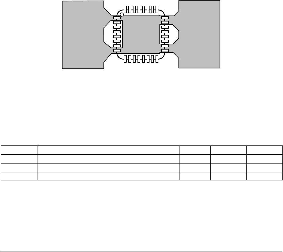
PACKAGE THERMAL CHARACTERISTICS
The 522 is available in a NQFP32 package. For cooling
optimizations, the NQFP has an exposed thermal pad which
has to be soldered to the PCB ground plane. The ground
plane needs thermal vias to conduct the heat to the bottom
layer. Figure 3 gives an example for good power distribution
solutions.
For precise thermal cooling calculations the major
thermal resistances of the device are given. The thermal
media to which the power of the devices has to be given are:
Static environmental air (via the case)
PCB board copper area (via the exposed pad)
The thermal resistances are presented in Table 5: DC
Parameters.
The major thermal resistances of the device are the Rth
from the junctiontoambient (Rthja) and the overall Rth
from the junctiontoexposed pad (Rthjp). In the table
below one can find the values for the Rthja and Rthjp,
simulated according to JESD51:
The Rthja for 2S2P is simulated conform JEDEC JESD51
as follows:
A 4layer printed circuit board with inner power planes
and outer (top and bottom) signal layers is used
Board thickness is 1.46 mm (FR4 PCB material)
The 2 signal layers: 70 mm thick copper with an area of
5500 mm
2
copper and 20% conductivity
The 2 power internal planes: 36 mm thick copper with
an area of 5500 mm
2
copper and 90% conductivity
The Rthja for 1S0P is simulated conform JEDEC JESD51
as follows:
A 1layer printed circuit board with only 1 layer
Board thickness is 1.46 mm (FR4 PCB material)
The layer has a thickness of 70 mm copper with an area
of 5500 mm
2
copper and 20% conductivity
Figure 3. Example of NQFP32 PCB Ground Plane Layout in Top View (Preferred Layout at Top and Bottom)
NQFP32
ELECTRICAL SPECIFICATION
Recommended Operation Conditions
Operating ranges define the limits for functional
operation and parametric characteristics of the device. Note
that the functionality of the chip outside these operating
ranges is not guaranteed. Operating outside the
recommended operating ranges for extended periods of time
may affect device reliability.
Table 4. OPERATING RANGES
Symbol Parameter Min Max Unit
V
BB
Analog DC supply +6 +30 V
V
DD
Logic supply output voltage 4.75 5.25 V
T
J
Junction temperature 40 +172 (Note 5) °C
5. No more than 100 cumulative hours in life time above T
tw
AMIS30522, NCV70522
http://onsemi.com
6
Table 5. DC PARAMETERS
(The DC Parameters are Given for V
BB
and Temperature in Their Operating Ranges Unless Otherwise Specified)
Convention: Currents Flowing in the Circuit are Defined as Positive.
Symbol
Pin(s) Parameter Remark/Test Conditions Min Typ Max Unit
SUPPLY INPUTS
V
BB
V
BB
Nominal Operating Supply Range 6 30 V
I
BB
Total Current Consumption Unloaded Outputs 8 mA
I
BBS
Sleep Current in V
BB
(Note 7) Unloaded Outputs 100
mA
V
DD
V
DD
Logic Supply Output Voltage 4.75 5 5.25 V
I
Load
Maximum Output Current
6 V V
BB
8 V 15 mA
8 V V
BB
30 V 50 mA
I
DDLIM
Current Limitation 150 mA
I
Load_PD
Output Current in Power Down Mode 1 mA
POWER ON RESET (POR) (Note 10)
V
DDH
V
DD
Internal POR Comparator Threshold V
DD
Rising 3.85 4.20 4.55 V
V
DDL
Internal POR Comparator Threshold V
DD
Falling 3.85 V
V
DDHYS
Hysteresis Between V
DDH
and V
DDL
0.10 0.35 0.60 V
MOTOR DRIVER
I
MDmax,Peak
MOTXP
MOTXN
MOTYP
MOTYN
Max Peak Current Through Motor Coil T
J
= 40°C 1600 mA
I
MDabs
Absolute Error on Coil Current T
J
= 125°C 10 10 %
I
MDrel
Error On Current Ratio I
coilx
/I
coily
7 7 %
I
SET_TC1
Temperature Coefficient of Coil Current
SetLevel, CUR[4:0] = 0...27
T
J
160°C 240 ppm/K
I
SET_TC2
Temperature Coefficient of Coil Current
SetLevel, CUR[4:0] = 28...31
T
J
160°C 490 ppm/K
R
HS
OnResistance HighSide Driver,
(Note 9) CUR[4:0] = 0...31
V
BB
= 12 V, T
J
= 27°C 0.45 0.56
W
V
BB
= 12 V, T
J
= 160°C 0.94 1.25
W
R
LS3
OnResistance LowSide Driver,
(Note 9) CUR[4:0] = 23...31
V
BB
= 12 V, T
J
= 27°C 0.45 0.56
W
V
BB
= 12 V, T
J
= 160°C 0.94 1.25
W
R
LS2
OnResistance LowSide Driver,
(Note 9) CUR[4:0] = 16...22
V
BB
= 12 V, T
J
= 27°C 0.90 1.2
W
V
BB
= 12 V, T
J
= 160°C 1.9 2.5
W
R
LS1
OnResistance LowSide Driver,
(Note 9) CUR[4:0] = 9...15
V
BB
= 12 V, T
J
= 27°C 1.8 2.3
W
V
BB
= 12 V, T
J
= 160°C 3.8 5.0
W
R
LS0
OnResistance LowSide Driver,
(Note 9) CUR[4:0] = 0...8
V
BB
= 12 V, T
J
= 27°C 3.6 4.5
W
V
BB
= 12 V, T
J
= 160°C 7.5 10
W
I
Mpd
Pulldown Current HiZ Mode 1 mA
DIGITAL INPUTS
I
leak
DI, CLK
NXT, DIR
CLR, CS
Input Leakage (Note 8) T
J
= 160°C 0.5
mA
V
IL
Logic Low Threshold 0 0.75 V
V
IH
Logic High Threshold 2.20 V
DD
V
R
pd_CLR
CLR Internal Pulldown Resistor 120 280
kW
R
pd_TST
TST0 Internal Pulldown Resistor 3 8
kW
6. Current with oscillator running, all analogue cells active, SPI communication and NXT pulses applied. No floating inputs. Guaranteed by
design.
7. Current with all analogue cells in power down. Logic is powered but no clocks running. All outputs unloaded, no inputs floating.
8. Not valid for pins with internal Pulldown resistor
9. Characterization Data Only
10.POR is derived from V
DD
. For proper POR operation V
BB
needs to be minimal V
BB_min
.

AMIS30522C5222G

Mfr. #:
Manufacturer:
ON Semiconductor
Description:
Motor / Motion / Ignition Controllers & Drivers 800MA STEPPER DRVR
Lifecycle:
New from this manufacturer.
Delivery:
DHL FedEx Ups TNT EMS
Payment:
T/T Paypal Visa MoneyGram Western Union

Products related to this Datasheet