Characteristics P6KE
4/9 Doc ID 3068 Rev 7
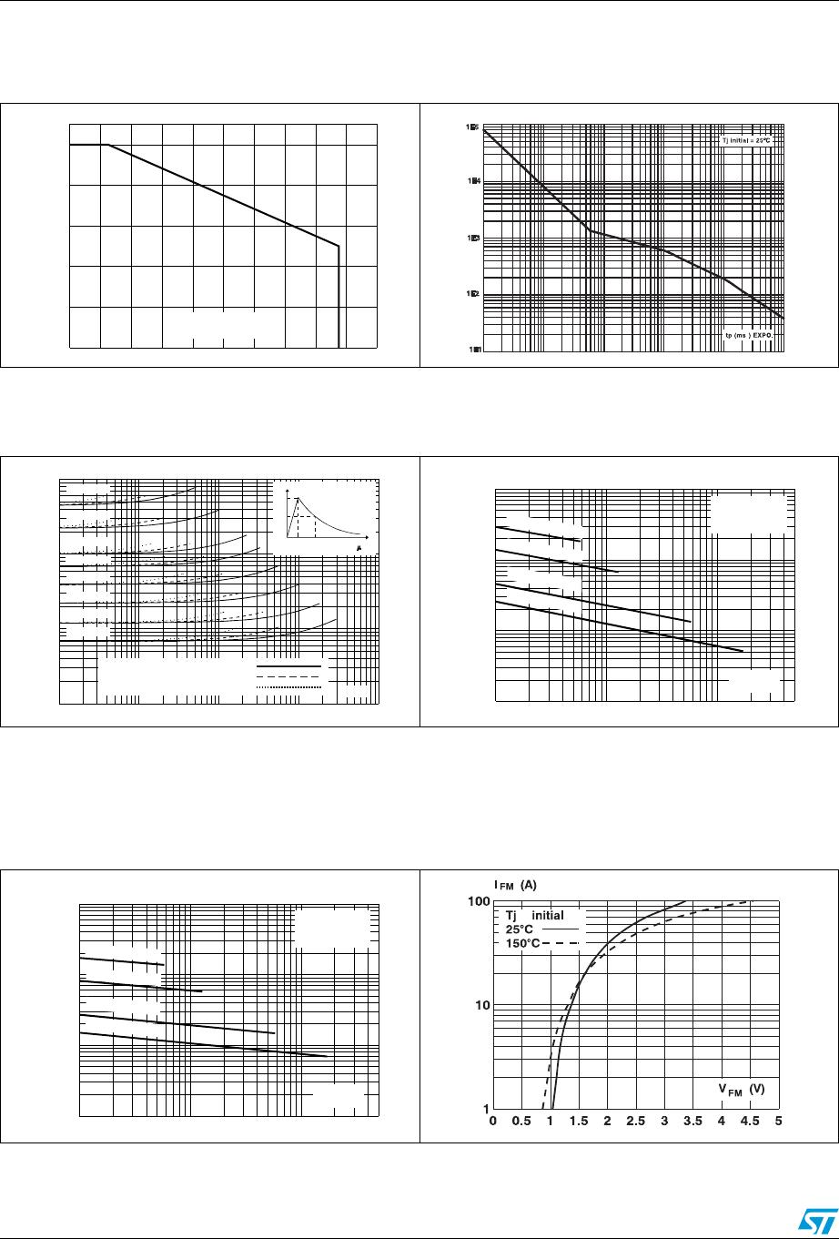
Figure 3. Peak power dissipation vs. initial
junction temperature
(printed circuit board)
Figure 4. Peak pulse power vs. exponential
pulse duration.
0
0
20
40
60
80
100
%
20
40 60 80 100 120 140 160 180 200
ø
Tj initial (°C)
0.001 0.01 0.1 1 10 100
Ppp
(W)
Figure 5. Clamping voltage vs. peak pulse
current
(1)
Figure 6. Capacitance vs. reverse applied
voltage for unidirectional types
(typical values).
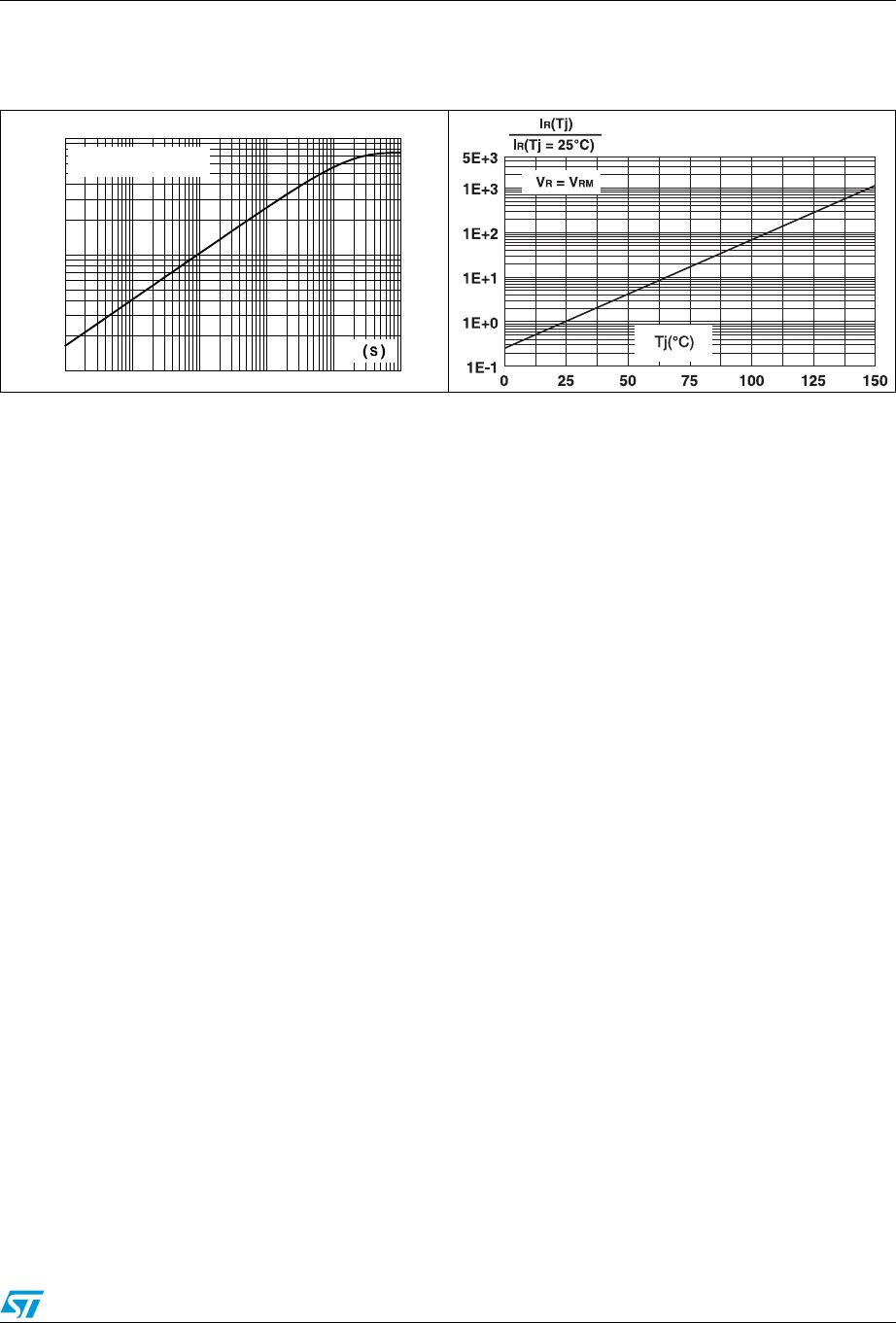
1. The curves in Figure 5 are specified for a junction temperature of 25°C before surge. The given results may be
extrapolated for other junction temperatures by using the following formula : ΔV
BR
= αT x [T
amb
-25] x V
BR
(25°C)
For intermediate voltages, extrapolate the given results.
0.1 1 10 100 1000
1
10
100
1000
V(V)
CL
Ipp (A)
t
%Ipp
100
50
0
t
r
t<10 s
r
t
Tj initial = 25øC
P6KE 440A
P6KE 220A
P6KE 68A
P6KE 39A
P6KE 22A
P6KE 12A
P6KE 6V8A
P6KE 100A
p
°
t = 20µs
p
t = 1ms
t = 10ms
p
p
Exponential waveform:
C (pF)
110100
10
100
1000
10000
V(V)
R
Tj = 25°Cø
F= 1 MHz
P
6
K
E
6
V
8
A
P
6
K
E
1
5
A
P
6
KE
6
8
A
P
6
K
E
2
0
0
A
5000
Figure 7. Capacitance vs. reverse applied
voltage for bidirectional types
(typical values).
Figure 8. Peak forward voltage drop vs. peak
forward current for unidirectional
types (typical value).
(1)
1. Multiply by 2 for units with V
BR
> 220 V.
5000
C (pF)
110100
10
100
1000
10000
V(V)
R
Tj = 25°Cø
F= 1 MHz
P
6
K
E
6
V8
C
A
P
6
K
E
1
5
C
A
P
6
K
E
6
8
C
A
P
6
K
E
2
0
0
C
A